In the intricate world of electronics, the Printed Circuit Board (PCB) is a fundamental component that acts as the foundation for electronic devices. From smartphones to medical devices, PCBs provide a platform for mounting and connecting electronic components. The complexity and functionality of a PCB are largely dictated by its layers. This article delves into the significance of PCB layers, their types, and how they contribute to the performance and design of electronic devices.
What are PCB layers?
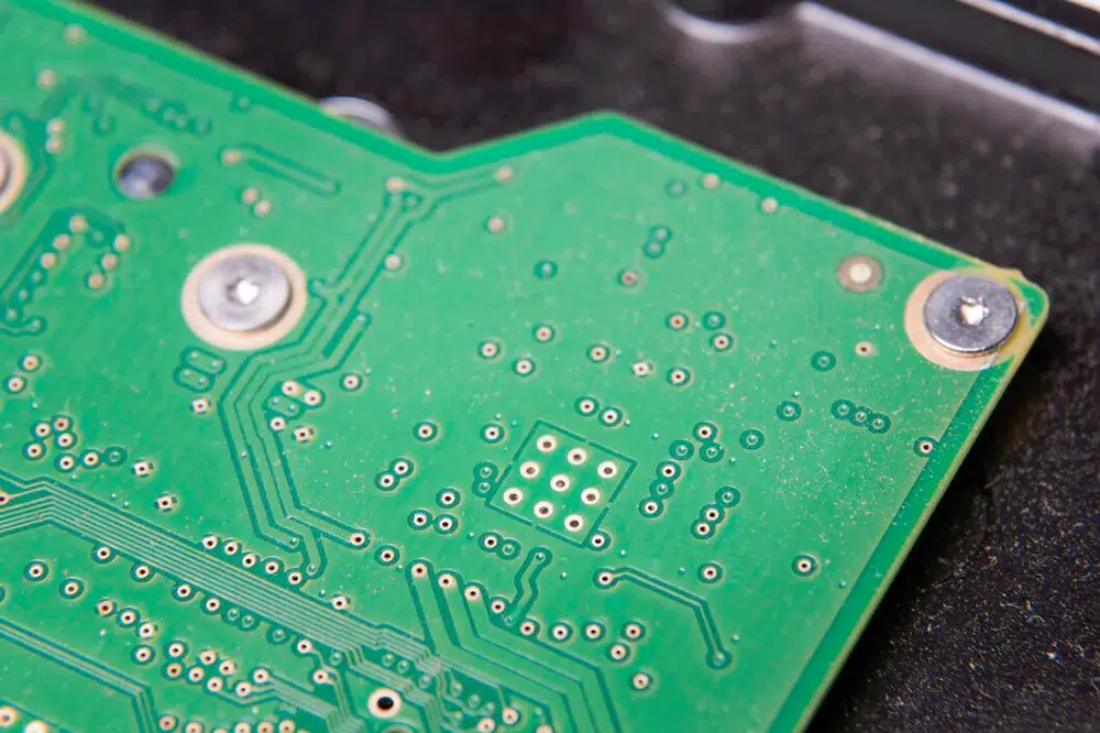
PCB layers refer to the different levels of conductive and insulating material that make up a printed circuit board. Each layer has a specific role, whether it be to carry electrical signals, provide structural support, or insulate different components. The layers are typically stacked together and laminated to form a single, functional board.
What are the types of PCB layers?
1. Single-Layer PCBs
– Definition: Also known as single-sided PCBs, these boards have one layer of conductive material (usually copper) and one layer of insulating material (such as FR4 fiberglass).
– Applications: Ideal for simple, low-cost electronics like calculators, power supplies, and some consumer electronics.
– Advantages: Easy to design and manufacture; cost-effective for low-volume production.
– Disadvantages: Limited in complexity and routing capabilities.
2. Double-Layer PCBs
– Definition: These boards have two layers of conductive material, separated by an insulating layer. Components can be mounted on both sides of the board.
– Applications: Common in more complex electronics, such as audio equipment and small computers.
– Advantages: Increased routing options and design flexibility compared to single-layer PCBs.
– Disadvantages: Slightly more expensive than single-layer PCBs and requires more complex manufacturing processes.
3. Multi-Layer PCBs
– Definition: Multi-layer PCBs consist of multiple layers of conductive material separated by insulating layers. These boards can have anywhere from three to dozens of layers.
– Applications: Used in high-performance applications like smartphones, tablets, and advanced medical devices.
– Advantages: High density of electronic components and connections, improved signal integrity, and reduced electromagnetic interference (EMI).
– Disadvantages: More expensive to manufacture and design due to increased complexity.
What are the PCB layers in multi-layer PCB?
1. Signal Layers
– These layers carry electrical signals between components. They can be designed for specific functions, such as analog signals, digital signals, or high-speed data.
2. Power Layers
– Dedicated to distributing power throughout the PCB, power layers ensure that electrical components receive the appropriate voltage and current. They often include planes for ground and various voltage levels.
3. Ground Layers
– Ground layers provide a common return path for electrical signals and help minimize noise and interference. They are crucial for maintaining signal integrity and ensuring stable operation.
4. Dielectric Layers
– Dielectric layers are insulating layers that separate conductive layers and prevent short circuits. They also affect the electrical performance of the PCB, including signal propagation speed and impedance.
Do PCB layers matter?
Yes, PCB layers are crucial to the performance and functionality of electronic devices. The number and arrangement of layers impact several key aspects:
Complexity and Routing: More layers allow for more complex circuit designs. Multi-layer PCBs can accommodate more routing paths and connections, which is essential for densely packed and high-performance electronics.
Signal Integrity: Proper layer configuration helps maintain signal integrity by reducing noise and electromagnetic interference (EMI). For high-speed signals, having dedicated signal layers and ground planes can prevent signal degradation.
Thermal Management: The ability to manage heat is critical, especially in high-power or high-density applications. Layering can facilitate better thermal dissipation by incorporating thermal vias or dedicated heat-sinking layers.
Size and Form Factor: More layers enable compact designs by stacking layers vertically rather than expanding the PCB horizontally. This is particularly useful for portable or space-constrained devices.
Cost and Manufacturing: The number of layers affects the cost of manufacturing and assembly. Single-layer boards are cheaper to produce than multi-layer ones. However, multi-layer boards can often provide better performance and reliability, justifying the additional cost.
How to identify the PCB layer?
Identifying PCB layers involves examining the board’s design and construction. Here are methods to determine the layers:
Visual Inspection:
Single-Layer and Double-Layer Boards: These are relatively straightforward to identify by looking at the top and bottom of the board. Double-layer boards will have components on both sides.
Multi-Layer Boards: For multi-layer boards, you might need to look at the board’s cross-section.
This can be done using X-ray inspection or a PCB cross-sectioning tool, which reveals the internal layers.
Documentation:
Gerber Files: These are the standard files used in PCB manufacturing. They include detailed information about the layers and their layout. Reviewing the Gerber files can provide insights into the number and arrangement of layers.
PCB Design Files: Tools like Eagle, KiCad, and Altium Designer offer ways to visualize and manage layers within the design software.
Manufacturer’s Specifications:
PCB manufacturers provide specifications and stack-up diagrams that outline the layers, materials, and their order. This information is crucial for understanding the construction of the board.
How do you decide on your PCB layer ordering?
Deciding on the layer ordering is a critical aspect of PCB design that affects both performance and manufacturability. Here’s how to approach it:
Define Requirements:
Signal Integrity: Determine the need for dedicated signal layers, especially for high-speed or sensitive analog signals. Place these layers between ground or power planes to shield them from interference.
Power Distribution: Decide how to distribute power across the board. Power layers (or planes) should be designed to handle the current demands and minimize voltage drops.
Consider Thermal Management:
Heat Dissipation: Plan layers to help with heat dissipation. Use thermal vias and place heat-generating components near thermal planes to effectively spread and dissipate heat.
Plan for Mechanical Support:
Structural Integrity: Ensure that the PCB’s structural needs are met, especially for mechanically stressed or large boards. The order of layers can contribute to the rigidity and stability of the board.
Optimize Manufacturing:
Cost and Complexity: Balancing cost and complexity is essential. While more layers can improve performance, they also increase manufacturing costs. Design layers to maximize performance within budget constraints.
Design for Testability and Maintenance:
Accessibility: Arrange layers to allow for effective testing and troubleshooting. Keep critical signals accessible and ensure that diagnostic tools can easily probe the necessary points.
Follow Best Practices:
Layer Stack-Up Guidelines: Adhere to established best practices for layer stack-up, such as placing ground and power planes close to signal layers and maintaining appropriate layer spacing.

Design Considerations for PCB Layers
1. Signal Integrity
– The arrangement and quality of the layers affect signal integrity. Proper layer stacking and routing minimize interference and signal degradation.
2. Thermal Management
– Multi-layer PCBs can generate significant heat. Effective thermal management strategies, such as incorporating thermal vias and heat sinks, are essential to prevent overheating.
3. Manufacturing Costs
– The complexity of the layer structure impacts manufacturing costs. While multi-layer boards offer advanced features, they are more expensive to produce.
4. Design Rules
– Designing PCBs involves adhering to specific rules for layer spacing, trace width, and hole placement. These rules ensure that the board functions correctly and can be manufactured reliably.
Conclusion
PCB layers are more than just an architectural detail; they are critical to the performance, reliability, and cost of electronic devices. From the straightforward single-layer designs to the complex multi-layer configurations, each type of PCB layer serves a unique purpose and addresses specific design requirements. Understanding these layers and their functions enables engineers to create more efficient and effective electronic products, pushing the boundaries of technology and innovation.
PCB layers refer to the different levels of conductive and insulating material that make up a printed circuit board. Each layer has a specific role, whether it be to carry electrical signals, provide structural support, or insulate different components.
Signal Layers
Power Layers
Ground Layers
Dielectric Layers
Complexity and Routing
Signal Integrity
Thermal Management
Size and Form Factor
Cost and Manufacturing

