Learn about definition and distinction of PCB, PCBA, SMT, HDI, UHDI, SPL and IC carrier board.
PCB(Printed Circuit Board)
Definition:
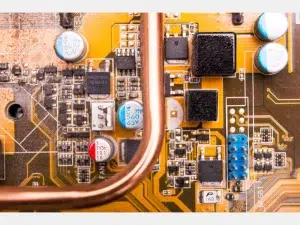
A printed circuit board (PCB) is a carrier used to support and connect electronic components. It uses conductive patterns to replace traditional wire connections, making the connection of electronic components simpler and more efficient. PCB is mainly composed of insulating substrate, conductive patterns, through holes, etc.
Category:
Based on differences in number of layers, structure and materials, PCB can be divided into single-layer, double-sided, multi-layer PCB boards, etc. In addition, there are special types such as flexible printed circuit boards (FPC) and high-frequency printed circuit boards (RF PCB).
Production process:
The production process of PCB includes design, plate making, manufacturing process, testing and other links. The design stage requires drawing the PCB layout based on the circuit schematic; the pattern making stage involves converting the designed layout into a physical entity; the manufacturing stage involves multiple process operations, such as PCB etching, drilling, gold plating, etc.; and finally, testing ensures the quality of the PCB .

PCBA(Printed Circuit Board Assembly)
Definition:
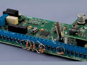
Printed circuit board assembly (PCBA) refers to the process of installing electronic components onto a printed circuit board and completing subsequent processes such as welding. Simply put, PCBA refers to a PCB that has completed component assembly.
Category:
PCBA can be divided into manual assembly and machine assembly. Manual assembly is suitable for small batch, multi-variety production and mainly relies on the skills of operators; while machine assembly uses automated equipment for component placement and is suitable for mass production.
Assembly process:
The assembly process of PCBA mainly includes patching, plug-in, welding and testing. SMT is the process of installing surface mount components (SMD) onto PCB; plug-in is the process of installing direct plug-in components onto PCB; soldering includes wave soldering, reflow soldering and other methods, which are used to fix components and PCB connection; the testing link is to ensure the performance and quality of PCBA.
SMT(Surface Mount Technology)
.webp)
Definition:
Surface mount technology (SMT) is an assembly technology that directly mounts surface mount components (SMD) on printed circuit boards. Compared with traditional plug-in technology, SMT has the advantages of higher assembly density, smaller size and faster production speed.
Category:
SMT is mainly divided into two links: patch and soldering. The patch link includes equipment such as patch machines, patch trays, and patch molds; the sldering link involves processes such as reflow soldering and wave soldering.
Process:
The SMT process mainly includes solder paste printing, patching, reflow soldering and inspection. Solder paste printing is the process of printing solder paste onto the PCB; patch placement is to place the SMD components in the correct position; reflow soldering melts the solder paste through heating to achieve welding of the components and the PCB; the inspection process includes visual inspection, Methods such as automated optical inspection (AOI) and X-ray inspection are used to ensure welding quality.
HDI board(High Density Interconnector)
A circuit board with a relatively high circuit distribution density using micro-blind buried via technology. The HDI board has inner and outer circuits, and processes such as drilling and in-hole metallization are used to connect the circuits in each layer internally.
HDI boards are generally manufactured using the lamination method. The more times there are laminations, the higher the technical grade of the board. Ordinary HDI boards are basically one-time lamination, while high-end HDI uses two or more lamination technologies, as well as advanced PCB technologies such as hole stacking, electroplating hole filling, and laser direct drilling.
There are currently four main types of HDI motherboards: first-order, second-order, third-order, and Any layer HDI. From front to back, the feature size gradually shrinks, and manufacturing becomes more and more difficult. Currently on the market, third-level, fourth-level or Any layer HDI motherboards are most commonly used in electronic terminal products. Currently, the Any layer that is widely used in electronic terminal products is 10-layer or 12-layer.
HDI(Ultra HDI)
As major countries around the world include chips and advanced packaging in their national development strategies, Ultra HDI has also received more and more attention. UHDI’s line width and line spacing, media thickness, and micropore aperture are one level higher than the current conventional HDI.
The existing IPC standards working group has proposed a new concept of ultra-high density interconnection (UHDI). The wire width and spacing of the UHDI board are less than 50μm, the interlayer dielectric thickness is less than 50μm, and the microvia diameter is less than 75μm.
Its performance exceeds the existing IPC 2226 HDI board level C; the UHDI structure is a convergence of similar carrier boards (SLP) and IC packaging The carrier board realizes the transition of line width and spacing from 40μm to 20μm, and the production technology changes from the subtractive method and the improved semi-additive method (mSAP) to the semi-additive method (SAP).
SLP(substrate-like PCB)
It is the main force of the next generation of PCB boards. Compared with HDI boards, it can be more detailed and can shorten the line width/line spacing from HDI’s 40/50 microns to 20/35 microns. From a process perspective, SLP is more It is close to the IC carrier board used for semiconductor packaging, but it has not yet reached the specifications of the IC carrier board. Its purpose is still to carry various active and passive components, so it still belongs to the category of PCB. The number of electronic components carried in the same area can be twice the number carried by HDI.
IC Package Substrate
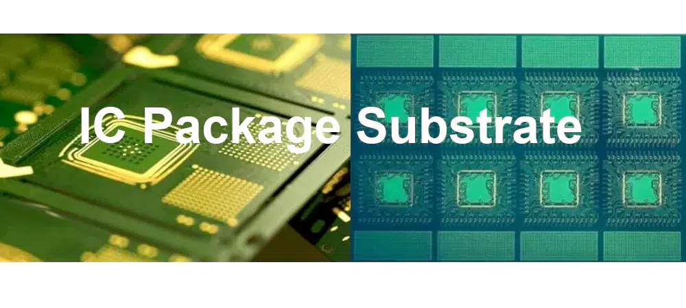
It is a key carrier in the packaging and testing process. It is used to establish the signal connection between the IC and the PCB. In addition, it can also protect the circuit, fix the circuit and dissipate waste heat. As a high-end PCB board, IC carrier board has the characteristics of high density, high precision, miniaturization and thinness.
In the field of high-end packaging, IC carrier boards have replaced traditional lead frames and become an indispensable part of chip packaging, not only providing support, heat dissipation and protection for chips.
At the same time, it provides electronic connections between the chip. What’s special is that almost all aspects involved in the packaging of integrated circuits are performed on or related to the IC carrier board.
Among the four basic technologies involved in electronic packaging engineering, namely thin and thick film technology, micro-interconnection technology, substrate technology, sealing and packaging technology, substrate technology is in a key and core position.
With the emergence of new high-density packaging forms, many functions of electronic packaging: such as electrical connection, physical protection, stress relaxation, heat dissipation and moisture resistance, size transition, standardization, standardization, etc., are gradually being partially or fully borne by the packaging substrate.
IC carrier boards are roughly divided into three categories according to different materials:
Rigid substrate: The main materials are: BT/ABF/MIS; its main application areas are: communication and memory chips, LED chips/CPUs, GPUs and chipsets, etc., a large number of high-end chips/analog, power IC, and digital currency and other market fields .
Flexible substrate: The main material is: PI/PE; its main application areas are: automotive electronics, consumer electronics and can also be used in launch vehicles, cruise missiles, space satellites and other military applications.
Ceramic substrate: The main materials are: aluminum oxide/aluminum nitride/silicon carbide; and the application fields are: semiconductor lighting, laser and optical communications, aerospace, automotive electronics, deep-sea drilling, etc.

