Welcome to the fascinating world of PCB pads. These tiny entities are nothing short of vital cogs in the expansive machine that is a PCB, providing the essential connection points that allow electronic components to interact and communicate. Despite their small size, their impact on circuit functionality is monumental.
In this guide, we will embark on a detailed exploration of PCB pad design, delving into its nuances and complexities and the profound role it plays in ensuring a successful and efficient electronic design. So, let’s embark on this journey together; after all, every great circuit starts with a single pad.
What is a PCB Pad?
A PCB pad, or Printed Circuit Board pad, is a fundamental element in electronics design. It’s essentially a region of copper on a PCB to which surface-mount components are soldered. Acting as a conduit, a PCB pad enables the flow of electrical signals between the board and the components.
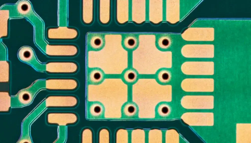
A PCB pad has several functions within the circuit, including the following:
- Electrical connections.
- Component attachment.
- Heat dissipation.
- Mechanical support.
- Signal routing.
Types of PCB Pad?
There are several variants of PCB pads, including the following:
- Non-plated pads. They have no copper plating in their holes. Used where electrical continuity between layers is not paramount.
- Test pads. Ideal for testing and troubleshooting.
- Via pads. Transitions connections or signals from one layer to the next.
- Castellated pads. Ideal when a PCB needs to be soldered directly to another PCB.
- Thermal pads. Designed to boost thermal performance by transferring heat away from components generating it efficiently.
- Surface-mount pads. Soldered onto the PCB’s surface. There are different types of surface-mount pads, including rectangular pads, gull-wing pads, J-Lead pads, Ball Grid Array pads.
- Through-hole pads. Used with through-hole components and are normally circular or oval and connected to copper traces.

What Is Pad Size in PCB?
In PCB design, pad size is a critical aspect that often requires careful consideration. The term “pad size” refers to the dimensions of the copper area where components are soldered onto the PCB. These pads act as the physical anchor points for components and form the electrical connections between these components and the circuit board’s traces.
The size of the pad can significantly influence the ease of soldering and the overall reliability of the board. It’s a delicate balance: too small a pad may result in inadequate solder joints, while an excessively large pad might lead to unnecessary consumption of board space and inefficient design.
Here’s what you need to consider for pad size in PCB design:
- Component orientation.
- Pad shape.
- Design rules.
- Thermal considerations.
- The manufacturing process.
- Lead spacing.
- Package style.
- Component type.
What Are PCB Pads Made Of?
Typically, a PCB pad is made of metal. The surface finish of the PCB pad will, however, depend on the specific requirements and intended use. Common metals that manufacturers use on any standard PCB pad include the following:
- Electroless Nickel Immersion Gold (ENIG). Has an electroless nickel layer and gold layer.
- Immersion Tin. Used in applications requiring flat and solderable surfaces.
- Immersion Silver. Suitable for fine-pitch components.
- Nickel. Enhances durability and solderability. Prevents the diffusion of copper into a gold surface.
- Silver. Used in specialized applications.
- Gold. Used in applications that require high performance and high reliability. It has superb corrosion resistance and maintains low contact resistance over time. It is ideal for critical components.
- Tin-Lead Alloy. Otherwise known as solder, it is especially common in through-hole components.
- Copper. Not only is it readily available, but also offers superb electrical conductivity.
What Is the Difference between Pad and via in PCB?

A PCB via and a PCB pad are two things that have different roles and characteristics. The primary differences include the following:
Function
A PCB pad creates a connection point to attach electronic components through mechanical or soldering means. A Via is a through-hole that links one layer of the PCB to another.
Appearance
A PCB pad is typically flat, rectangular, or circular. Vias are cylindrical holes passing through the PCB, which connect one layer to the other. Vias can be either through-hole or blind.
Purpose
Pads are used for component attachment while Vias are ideal for signal routing.
Design Considerations
A PCB pad is designed depending on the component size, type, and spacing. This is why they are unique to their components. On the other hand, Vias are designed based off of their size, purpose, and placement.
Electrical Role
Pads mainly serve an electrical function since they establish a connection between the component and PCB traces. They are ideal for electrical continuity. Vias, on the flip side, play an electrical role by permitting signals to move between layers. They help to maintain electrical connectivity.
How Do You Choose a Pad Size?
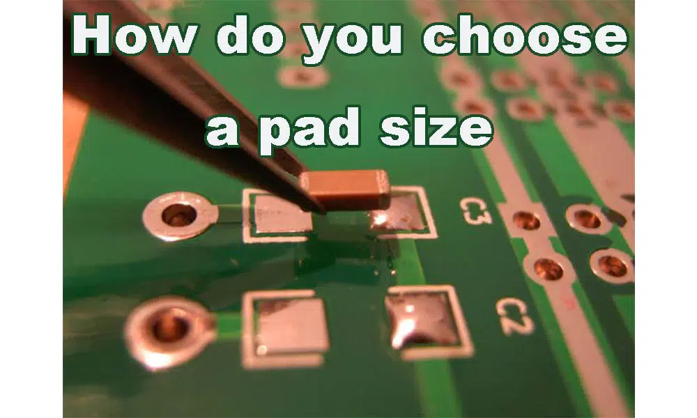
Here’s how to choose a PCB pad size:
1. Identify the component type.
2. Check the component datasheets.
3. Consider the lead pitch.
4. Account for tolerances.
5. Follow the design rules.
6. Thermal considerations.
7. Consider the manufacturing procedure.
8. Perform tests and prototyping.
9. Consider IPC standards.
10. Seek advice from an industry expert.
How To Repair Damaged PCB Pad?
To repair a damaged PCB pad, here’s what you will need:
- Solder mask repair pen (optional).
- Flux.
- Heat-resistant tape.
- Copper wire or foil.
- Epoxy or super glue.
- Abrasive pad or fine-grit sandpaper.
- Multimeter.
- Desoldering tools.
- Soldering station and soldering iron.
The steps to follow when repairing a damaged PCB pad include the following:
1. Assess the damage.
2. Ensure you follow safety precautions.
3. Remove any necessary components.
4. Clean the area.
5. Repair the pad.
6. Reconnect any removed components.
7. Test using a multimeter to ensure continuity.
8. Clean and inspect.
9. Apply the solder mask (optional).
Where to Buy PCB Pad?
Here’s where you can buy a PCB pad:
- Online marketplaces like Alibaba, Amazon, eBay, etc.
- Local electronic shops.
- Online PCB design software and services.
- Electronic distributors.
- PCB assembly services.
- PCB manufacturers.
Final Thoughts
In conclusion, mastering the fundamentals of PCB pad design plays a key role in obtaining optimal performance from your printed circuit boards. PCB pads are not merely points of connection; they represent the groundwork upon which reliable, high-performing electronic devices are built.
At IBE, we understand this and hold it at the heart of our services. Our empathetic and professional team taps into their creativity while adhering to industry standards to ensure that your PCB designs are structurally sound and fit for their intended applications. Remember, a well-executed PCB pad design contributes to a successful PCB project, and with IBE, you are assured of that success. Choose us for your PCB pad design needs—because we’re not just experts, we’re your partners in innovation.
A PCB pad, or Printed Circuit Board pad, is a fundamental element in electronics design. It’s essentially a region of copper on a PCB to which surface-mount components are soldered. Acting as a conduit, a PCB pad enables the flow of electrical signals between the board and the components.
- Non-plated pads.
- Test pads.
- Via pads.
- Castellated pads.
- Thermal pads.
- Surface-mount pads.
- Through-hole pads.
In PCB design, pad size is a critical aspect that often requires careful consideration. The term “pad size” refers to the dimensions of the copper area where components are soldered onto the PCB. These pads act as the physical anchor points for components and form the electrical connections between these components and the circuit board’s traces.

