As electronic products advance, PCBs must progress in precision, materials and fabrication techniques to fulfill more complex demands.
This article explores what exactly PCB fabrication involves, methods utilized, specialized equipment, essential base materials, and considerations when selecting a fabrication partner to produce quality boards.
Understanding the manufacturing processes transforming circuit designs into functional reality facilitates smarter decisions ensuring product integrity.
What Is PCB Fabrication?
PCB fabrication is the process of physically constructing conductive copper traces and pads on an insulating substrate base according to an electronic circuit design.
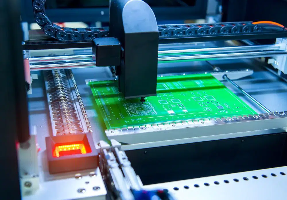
PCB fabrication transforms design files into functional boards ready for electronics assembly and soldering.

What is the Difference Between PCB Manufacturing and Fabrication?
While often used interchangeably, PCB manufacturing refers to the full end-to-end sequence of processes from initial circuit design, simulation, prototyping, fabrication, assembly, and testing to complete electronic products.
PCB fabrication focuses specifically on the core construction of the printed circuit board layered materials. It is one crucial stage within the overall manufacturing continuum.
What are PCB Fabrication Methods?
There are several common PCB fabrication methods:
Subtractive Fabrication
The most prevalent method starts with a blank copper-clad laminate substrate that gets selectively etched away to leave just the desired conductive pattern on the base. Most traditional PCB fabrication relies on well-refined subtractive processing.
Additive Fabrication
This method builds up circuit traces by electroplating additional copper material only where conductive paths are needed onto an initially unclad substrate. Additive processing minimizes wasted conductive materials but requires more complex processing gear.
Semi-Additive Fabrication
As its name indicates, semi-additive fabrication combines aspects of both fully additive and subtractive processes, first selectively electroplating a thin copper foil layer onto substrates before etching away unwanted areas to leave the circuit layout behind. This approach provides finer trace control than pure subtractive techniques.
Metal Core PCBs
Alternate metal core substrates like aluminum or copper alloys get used as the core rather than insulating bases for very high thermal conductivity demands. Dielectric separation layers isolate mounted electronics from the conductive substrate which serves as an integral heat spreader.
High-Density Interconnect (HDI) PCBs
This advanced technique fabricates extremely compact yet complex PCBs through sequentially bonding together thin layers of flexible circuit substrates with microvias. HDI stacking attains far greater layout densities than possible with conventional fabrication to minimize product form factors. Because of the delicacy of layered structures, laser micromachining and precise dry-film lamination processes become essential.
What is the PCB Fabrication Process?
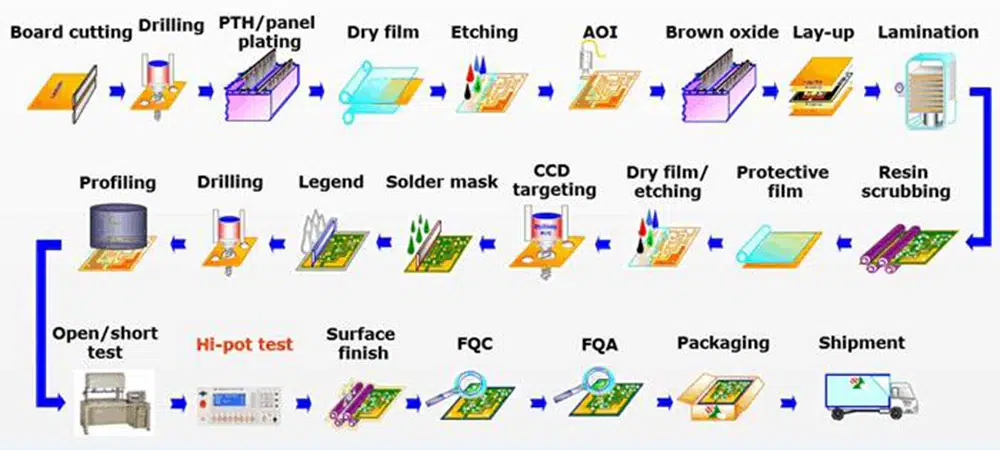
A typical rigid glass reinforced epoxy laminate FR-4 printed circuit board gets made subtractively through several key process stages including:
1. Conductive copper foil, typically 1⁄2 to 2 oz thickness, gets laminated onto insulating woven fiberglass composite substrates using heat and adhesive films to form panel sizes suitable for further processing.
2. Precise photoresist coatings are applied over copper layers then selectively exposed to high intensity UV light through custom artwork film patterns.
3. Exposed photoresist gets chemically developed and washed away, revealing areas of raw copper traces to be eventually etched away while the remaining photoresist shields desired conductive paths.
4. Etchant solutions aggressively cut into unprotected copper regions, effectively isolating delicate circuit paths as defined during prior photoresist exposure and development while copper below protective photoresist stays intact.
5. All remaining photoresist gets finally stripped away in preparation for automated optical inspection and electrical testing before further fabrication processing.
6. High precision mechanical drilling machines cut into panel materials to create holes needed for conductive vias and mounting component terminations.
7. Electroless copper and/or direct electroplating coat drilled holes to efficiently facilitate interlayer connectivity through the entire finished board thickness before they get squeezed together.
8. Outer-layer circuitry panels undergo final fusion bonding under heat and pressure with prepreg or polyimide bonding sheets into multilayer composite structures.
9. Panels ultimately get routed into individual printed circuit boards then exhaustively tested against fabrication quality standards before shipment or assembly.
What are the PCB Fabrication Machines?
Integrated automated production lines form the core of printed circuit board manufacturing facilities by efficiently moving panel materials sequentially between specialized fabrication process stations including:
Lamination Presses: Apply tons of heat and pressure to fuse together insulating and conductive layers into panel form factors.
Exposure Units: Transmit high-intensity ultraviolet light through custom artwork film masks to transfer microscopic circuit image patterns onto the photoresist.
Etchers: Remove unwanted copper metal not protected by photoresists through immersion chemical baths.
Hole Drills: Use carbide bits to cut into panel materials creating holes needed for electrical connectivity between layers and component lead insertions.
Routers: Trim fabricated panels down into individual rectilinear printed circuit boards by cutting through the entire finished thickness.
Automated Optical Inspection (AOI) Units: Validate quality standards, registration alignments, and test for electrical connectivity faults.
What are the PCB Fabrication Materials?
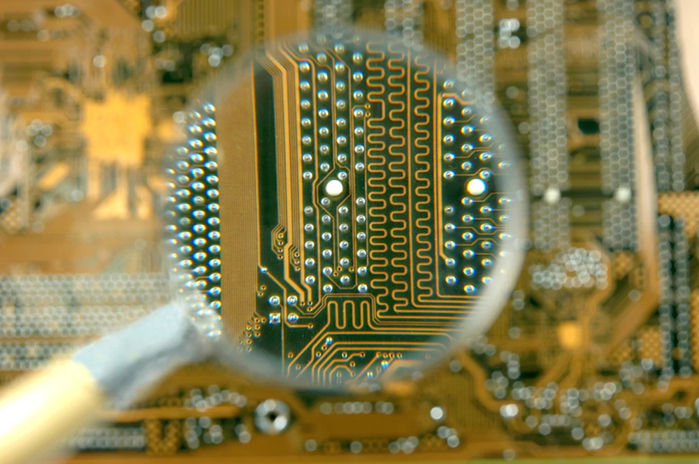
Basic rigid laminate PCB fabrication materials include:
Substrate – Base insulating core such as FR-4, CEM-1, and polyimides provide foundations onto which circuits get built
Conductive Metal Foils: Copper alloys form over 98% of all PCB traces and pads due to high conductivity and proven processing reliability, along with some applications utilizing aluminum, nickel silver or resistive materials
Bonding Films: FR-4 or polyimide prepreg sheets coated with partially cured epoxy resins fuse together layers with heat
Photoresists: Temporary acrylate polymer coatings facilitate image transfer of circuit layouts
How to Choose a PCB Fabrication Manufacturer?
Carefully choosing a PCB fabrication partner with proven expertise ensures professionals optimally construct your boards right the first time meeting stringent tolerance and testing specifications critical for mission-critical electronics reliability and performance.
Factors to evaluate include:
●Diverse range of PCB technology capabilities suited to application-specific requirements
●Operations quality certifications like IATF 16949, ISO 9001 affirming adherence to respected manufacturing standards
●Design for Manufacturability (DFM) advisory resources to review and optimize PCB data packs during development
●Competitive fabrication costs for delivered production quality, not just prototypes but across low to high-volume batches
●Responsive application engineering support to ensure your program success
Conclusion
As electronic products continue trending smaller and more powerful, the interconnect foundations fabricated with intricacy and precision play an increasingly vital role. PCB fabrication leverages a range of specialized processes, automations, and material science advancements striving for reliable quality across economies of scale.
Subtractive methods retain dominance today by refining decades of expertise in cost-effective high volume manufacturing. Yet innovations in additive, semi-additive, and advanced stacking fabrication unlock new possibilities as complexity demands escalate further.
By understanding the capabilities existing between circuit design art and physical board production science, engineers can craft optimized next-generation products pushing further into immense technological possibilities ahead.
PCB fabrication is the process of physically constructing conductive copper traces and pads on an insulating substrate base according to an electronic circuit design.
While often used interchangeably, PCB manufacturing refers to the full end-to-end sequence of processes from initial circuit design, simulation, prototyping, fabrication, assembly, and testing to complete electronic products.
PCB fabrication focuses specifically on the core construction of the printed circuit board layered materials. It is one crucial stage within the overall manufacturing continuum.
- Subtractive Fabrication
- Additive Fabrication
- Semi-Additive Fabrication
- Metal Core PCBs
- High-Density Interconnect (HDI) PCBs

