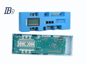
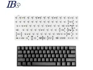
PCB layout is a crucial step in electronic design, influencing the performance, reliability, and manufacturability of the circuit board. The PCB layout should follow principles such as placing critical components first, followed by smaller components, partitioning the circuit according to its functionality, and maintaining signal integrity.
PCB Routing should control trace lengths, avoid sharp corners and right angles, and appropriately set trace widths and layer routing. Additionally, considerations should be made for thermal design, maintainability, electromagnetic compatibility, and testability. Adhering to these rules and considerations ensures the quality and performance of PCB layout, enhancing the overall performance of electronic systems.
Steps of Board Layout
1. Determine PCB Size and Layers: Based on the requirements of the circuit design, determine the size and number of layers of the PCB.
2. Import Netlist: Import the netlist of the circuit design into the PCB design software as a basis for layout.
3. Preliminary Component Placement: Pre-layout of components based on circuit functional partitioning and priority layout principles.
4. Routing Design: Based on the layout of components, perform routing design, paying attention to signal integrity, power stability, and routing reliability.
5. Optimization Adjustment: Optimize and adjust the layout and routing to ensure that the PCB performance reaches the best state.
Rules of Board Layout
Place Critical Components First: First determine and place the most important components in the circuit, such as power supplies, processors, memories, etc., as well as high-frequency or high-speed components.
Start with Large, then Small; Start with Difficult, then Easy: Place important unit circuits and core components first, giving priority to larger and more complex components to ensure reasonable layout of critical parts.
Partition According to Circuit Function: Layout according to the functional modules of the circuit, concentrating components with the same or similar functions for easier signal transmission and management.
Maintain Signal Integrity: For high-speed signal lines, avoid crossing with other signal lines or power lines to prevent signal crosstalk and interference. Layered layout can be used to place signal lines, power lines, and ground lines on different layers.
Component Arrangement: Large components should not be placed around small components, and there should be sufficient space around components that need debugging for easy maintenance and adjustment.
Thermal Management: Heat-generating components should be kept away from sensitive components, and ensure a good heat dissipation path to avoid heat accumulation.
Even Distribution, Balanced Center of Gravity: Follow the principle of even distribution to make the layout aesthetically pleasing, while maintaining a balanced center of gravity to avoid uneven stress on the PCB due to center of gravity deviation.
Consistent Orientation for Components of the Same Type: Components of the same type should be placed in the same direction in the X or Y direction for ease of production and inspection.
Rules of PCB Routing
Control Trace Lengths: Try to shorten trace lengths as much as possible, especially for critical signal lines, to reduce signal attenuation and delay.
Avoid Sharp Corners and Right Angles: When routing, avoid sharp corners and right angles, and try to use rounded corners or angles of 45 degrees to reduce signal reflections and impedance mismatches.
Trace Width: Determine trace widths based on current requirements and thermal considerations to ensure circuit reliability and stability.
Interlayer Routing: Make reasonable use of interlayer routing in multilayer PCBs, such as placing signal lines on inner layers and power and ground lines on outer layers.
Impedance Control: For high-speed signals, impedance control is necessary to ensure signal integrity, and impedance matching designs may be required when necessary.
Avoid Crossings and Parallel Routing: Try to avoid signal line crossings and parallel routing to reduce crosstalk and electromagnetic interference.
Decoupling Capacitors: Place decoupling capacitors near power supply pins to filter out high-frequency noise and stabilize the power supply.
Considerations
• Thermal Design: Consider thermal design to prevent circuit performance degradation or damage due to overheating.
• Maintainability: Consider maintainability during layout to facilitate future repairs and upgrades.
• Electromagnetic Compatibility (EMC): Consider EMC during routing to minimize the possibility of interference and crosstalk.
• Testability: Ensure ease of testing and verification for future diagnostics.
Other Tips
Via Usage: Minimize the use of vias, especially in high-frequency signals. If there are many traces, consider using multilayer boards.
Through-hole vs. Blind/Buried Vias: Through-holes are easier to implement in terms of process and lower cost, while blind/buried vias can increase the density of multilayer boards, reduce the number of layers, and decrease the board size.
Analog and Digital Hybrid Systems: Use electric layer division, adopt a full copper ground plane, or connect different grounds at the power source endpoints, depending on specific circumstances.
By following the above principles and considerations, the quality and performance of PCB layout can be ensured, thereby improving the performance and reliability of the entire electronic system. During the design process, it is also necessary to flexibly adjust and optimize the layout scheme according to specific application scenarios and requirements.

