Bipolar Junction Transistors (BJTs) are semiconductor devices that play a fundamental role in electronic circuits for amplification and switching applications. They are a type of transistor that utilizes both electron and hole charge carriers in a semiconductor to control the flow of current.
They have been widely used for amplification and switching applications since their invention in the 1950s. This article will discuss the working principle, characteristics, types, configurations and applications of Bipolar junction transistors.
What is a bipolar junction transistor and its characteristics?
A Bipolar Junction Transistor is a type of semiconductor device that acts as an amplifier or a switch in electronic circuits. It is constructed using three semiconductor layers and two pn-junctions. The three layers are called the emitter, base, and collector. There are two types of BJTs: NPN (Negative-Positive-Negative) and PNP (Positive-Negative-Positive), based on the arrangement of the semiconductor materials.
The key characteristics of a BJT are:
• It operates by the flow of both majority and minority charge carriers (holes and electrons), hence it is called a bipolar transistor.
• The current gain or amplification level can be changed by adjusting the base current.
• Bipolar junction transistors can operate in either active mode or switching mode based on the biasing conditions.
What are the two types of bipolar junction transistors?

The two main types of bipolar junction transistors are NPN and PNP. They are categorized based on the doping used in their semiconductor material.
A key difference between these two is the type of majority charge carriers.
NPN BJT:
An NPN transistor consists of an N-type semiconductor material sandwiched between two P-type semiconductor regions. Specifically:
• The emitter region is made of N-type semiconductor material, which is lightly doped with donor impurities like antimony or phosphorus. This makes free electrons the majority carriers in the emitter.
• The base region is made of a P-type semiconductor material, which is lightly doped with acceptor impurities like boron. This results in holes being the majority carriers in the base.
• The collector region is formed from a P-type semiconductor that is more heavily doped than the base. Holes are the majority carriers here as well.
PNP BJT:
A PNP transistor has the opposite doping – it consists of a P-type semiconductor sandwiched between two N-type materials. In this case:
• The emitter is made of a P-type semiconductor and holes are the majority carriers.
• The base is an N-type material with electrons as the majority charge carriers.
• The collector also uses an N-type material but with higher doping for increased conductivity.
In both types, the flow of either electrons or holes can be regulated by varying the base voltage to control signal amplification and device operation.
What is the basic construction of a bipolar junction transistor?
Bipolar junction transistors have a basic construction consisting of just three doped semiconductor regions forming the key terminals – emitter, base and collector. Specifically for an NPN transistor:
Emitter Region: This is a thin section of the transistor extended towards the front. It is heavily doped with donor or N-type impurities (such as arsenic or phosphorus) to make it highly conductive.
Base Region: Positioned between the emitter and collector regions, the base is very thin – usually less than 1 micrometer. It is lightly doped with acceptor or P-type impurities (such as boron).
Collector Region: Forming the back section of the BJT, the collector is heavily doped with P-type impurities to make it highly conductive. It has the largest surface area of the three regions.
These doped semiconductor regions are grown on a semiconductor substrate using metalorganic chemical vapor deposition or diffusion/ion implantation processes in the manufacturing of BJTs. Ohmic contacts made of alloyed metals provide the three terminal connections – emitter, base and collector.
Very thin insulating and passivation layers are deposited to cover the semiconductor surfaces and edges to avoid surface leakage currents. This simple heterojunction structure formed by the PN junctions enables the flow of electrons or holes between the regions based on applied biases, allowing usage as an amplifier or switch.

Why are bipolar junction transistors used?
BJTs are commonly used for the following purposes:
Amplification: Due to the current gain property, BJTs are extensively used to amplify signals in audio amplifiers, radio receivers, etc.
Switching: BJTs can be efficiently used as switches by applying certain biasing conditions in digital circuits.
Oscillators: BJTs aid in generation of oscillating signals for various applications when used in oscillator circuits.
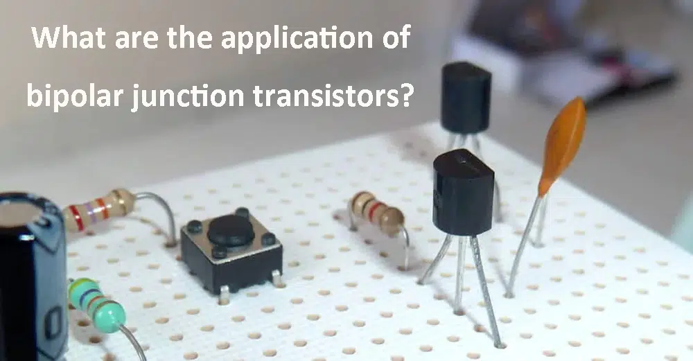
What are the application of bipolar junction transistors?
Audio Amplifiers: BJT audio amplifiers are widely used in home/car audio systems to amplify audio signals.
Radio Receivers: In the radio frequency (RF) stage of receivers, BJTs aid in signal amplification and mixing.
Digital Electronics: BJTs perform logic operations like AND, OR, NOT in digital circuits as electronic switches.
Temperature Sensors: BJT characteristics change with temperature, which is utilized in temperature sensing applications.
What is the difference between a BJT and a Mosfet?
1. BJTs use both electrons and holes as current carriers, whereas MOSFETs primarily use one type of charge carrier – electrons for NMOS and holes for PMOS.
2. BJT current flow is controlled by base current, while MOSFET current is controlled by gate voltage.
3. BJTs require a constant base drive current for operation, whereas no continuous DC current flows into the gate of a MOSFET.
4. BJTs have low input impedance and high output impedance, MOSFETs have high input impedance and low output impedance.
What are the different bipolar transistor configurations?
Common Base (CB): Input is at base, output is at collector, and power supply is at emitter. Used as a voltage amplifier.
Common Emitter (CE): Input is at base, output is at collector, and power supply is at collector. Most widely used configuration.
Common Collector (CC): Input is at base, output is at emitter, and power supply is at collector. Used as a current buffer.
What is the mode of operation of a bipolar junction transistor?
Bipolar junction transistors can be operated in two modes:
Active Mode: The transistor is forward biased used for amplification. It allows a small base current to control a much larger collector current.
Cut-off/Saturation Mode: The transistor is reverse biased used for switching applications. It acts as an open/closed switch.
What are the common troubles of bipolar junction transistors?
Thermal Runaway: Higher current flow caused by the increased temperature further raises temperature, leading to damage.
Leakage Currents: Junction or surface leakage causes unwanted low-level currents to affect performance.
Parasitic Effects: Stray inductance/capacitance causes problems like oscillations at high frequencies.
Secondary Breakdown: Beyond safe operating area, voltage across junctions triggers destructive breakdown.
Conclusion
In conclusion, the bipolar junction transistors are fundamental electronic devices having gain, switching and signal processing capabilities.
Bipolar junction transistors are the backbone of many electronic circuits.
Understanding the working of BJTs is crucial for the design and development of various electronic systems.
The BJT has made a huge impact in electronics and still holds importance regardless of the fact that MOSFETs have superior features for some applications.
BJTs continue to remain relevant and find application in some niche areas due to their simple design.
A semiconductor device that controls the flow of current in electronic circuits, acting as an amplifier or a switch.
NPN (Negative-Positive-Negative) and PNP (Positive-Negative-Positive).
It operates based on the principles of minority carrier injection, amplification, and the control of current flow between different semiconductor layers.

