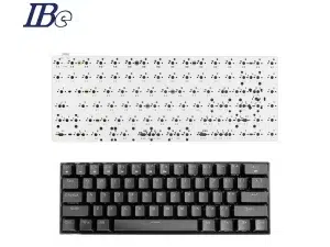
Copper clad laminate (CCL) is a critical material in the world of electronics, specifically in the production of printed circuit boards (PCBs). This composite material serves as the foundational substrate that supports and interconnects electronic components. In this article, we’ll explore what copper clad laminate is, its composition, types, and applications.
What is Copper Clad Laminate?
Copper clad laminate is a composite material that consists of a layer of copper foil bonded to a dielectric substrate. The dielectric substrate can be made from various materials, including epoxy resin, phenolic resin, or polyimide. The copper layer serves as the conductive pathway for electrical signals, while the substrate provides mechanical support and insulation.
What are the benefits of Copper Clad Laminate ?
Copper clad laminate is essential in modern electronics for several reasons:
1. Electrical Performance: The combination of copper and dielectric materials allows for efficient signal transmission and minimized electrical interference.
2. Mechanical Stability: CCL provides a robust substrate that can withstand thermal cycling, vibration, and physical stress.
3. Versatility: With various types of CCL available, manufacturers can choose the right material for specific applications, ensuring optimal performance.
4. Cost-Effectiveness: CCL is relatively inexpensive compared to other materials, making it an ideal choice for mass production.
What is Copper Clad Laminate made of?
CCL is typically made up of three main components:
1. Copper Foil: The copper layer varies in thickness, usually ranging from 0.5 oz/ft² to 6 oz/ft². Thicker copper is often used for high-power applications.
2. Dielectric Substrate: This material can be made from different resins, such as:
– FR-4: A widely used epoxy-based resin known for its excellent electrical properties and mechanical strength.
– Polyimide: Suitable for high-temperature applications and flexible PCBs.
– Phenolic: Generally used for lower-cost applications.
3. Adhesive Layer: An adhesive binds the copper to the substrate, ensuring a strong and durable bond that withstands the manufacturing processes.
What are the types of copper clad laminate?
There are various types of copper clad laminates, categorized based on their dielectric materials and applications:
1. Standard CCL: Typically made from FR-4, suitable for most general-purpose PCBs.
2. High-Frequency CCL: Used in RF and microwave applications, these laminates are made from materials like PTFE (Teflon) that minimize signal loss.
3. Flexible CCL: These are made from flexible substrates like polyimide, ideal for applications where bending and folding are required.
4. Metal Core CCL: Incorporates a metal core (usually aluminum or copper) for enhanced heat dissipation, used in LED lighting and power electronics.
What is copper clad laminate used for?
CCL is fundamental in various industries, including:
– Consumer Electronics: Smartphones, tablets, and laptops rely on PCBs made from copper clad laminates for their functionality.
– Automotive: With the rise of electric vehicles, advanced driver-assistance systems (ADAS), and infotainment systems, CCL plays a vital role in automotive electronics.
– Telecommunications: Infrastructure for wireless communication, including antennas and routers, utilizes high-frequency CCL.
– Medical Devices: Precision medical equipment requires reliable and compact PCBs, often made from specialized CCL.
How do you clean Copper clad laminate?
Cleaning copper-clad laminate (CCL) is important for preparing it for circuit board fabrication or repairs. Here’s how to clean it effectively:
1. Initial Dust Removal:
Use compressed air to blow off any loose dust or debris from the surface.
2. Soak in Soapy Water:
If there’s significant grime, soak the laminate in warm, soapy water for a few minutes. Use mild dish soap.
3. Gentle Scrubbing:
If needed, use a soft cloth or a gentle scrub brush to clean the surface. Be careful not to scratch the copper.
4. Rinse:
Rinse thoroughly with distilled water to remove soap residue.
5. Solvent Cleaning:
For any remaining residues, use isopropyl alcohol or acetone on a lint-free cloth to wipe the surface. This will help remove oils and other contaminants.
6. Drying:
Allow the laminate to air dry completely or gently dry it with a soft cloth. Ensure there is no moisture left before proceeding to use it.
How thick is the Copper clad laminate?
The thickness of copper-clad laminate (CCL) varies depending on the specific type and application, but it typically ranges from about **0.2 mm (8 mils)** to **3.2 mm (125 mils)**. Common thicknesses for CCL used in PCB manufacturing are:
– **0.8 mm (31.5 mils)**
– **1.6 mm (63 mils)** (most common)
– **2.0 mm (79 mils)**
These measurements include both the laminate material and the copper layers, so the overall thickness will depend on the specific configuration of the laminate used.
Conclusion
Copper clad laminate is a cornerstone of PCB manufacturing, enabling the functionality of countless electronic devices that we use every day. As technology continues to advance, the demand for high-performance, reliable CCL will only increase. Understanding its composition, types, and applications helps highlight the integral role it plays in the electronics industry and paves the way for future innovations. Whether in consumer electronics, automotive applications, or telecommunications, copper clad laminate remains an indispensable component of modern technology.
Copper clad laminate is a composite material that consists of a layer of copper foil bonded to a dielectric substrate.
Electrical Performance
Mechanical Stability
Versatility
Cost-Effectiveness
CCL is typically made up of three main components:
1. Copper Foil
2. Dielectric Substrate
3. Adhesive Layer

