In the PCB manufacturing process, the stencil is made to accurately coat the solder paste on the solder paste layer of the PCB board. In order to make a stencil, we usually use the solder paste layer, or called: “paste mask layer”.
A solder paste layer is a layer in a PCB design file that determines the location and shape of the solder paste. This layer will show where the solder paste needs to be placed before the PCB surface mount technology (SMT) components are soldered. During the soldering process, the stencil layer will cover the solder paste layer, and then through the holes on the stencil layer, the solder paste will be precisely apply to the PCB pad, so as to achieve accurate soldering in the subsequent component placing process.
Therefore, the solder paste layer is necessary to make stencil layer. In the early stage of PCB manufacturing, the information about solder paste layer is sent to the PCB manufacturer, and the manufacturer will generate corresponding stencil layer based on this layer to ensure the accuracy and reliability of soldering.
What is stencil layer ?
In PCB design, “Pastemask” (also known as “Solder Paste Mask” or “Solder Mask” for short) is an important layer. It is a key part of the soldering process used to assemble Surface Mount Devices (SMD).
The role of the stencil layer is to prevent the solder paste from being applied to areas that should not be soldered when soldering SMD components. Solder paste is a material used to connect SMD components and PCB pads, and the Pastemask layer acts as a “barrier” to ensure that paste can only be applied to specific soldering areas.
The design of the Pastemask layer is very important in the PCB manufacturing process, because it directly affects the soldering quality and overall performance of SMD components. When doing PCB design, designers need to carefully consider the layout of the Pastemask layer to ensure that it matches other layers (such as pad layers, component layers, etc.) to ensure the accuracy and reliability of the soldering process.

Design specifications for stencil layers
In PCB design and manufacturing, the process specification of the Solder Mask Layer is usually defined by industry standards and manufacturer’s requirements. The following are some common process specifications for solder paste layers:
IPC-SM-840C: This is the solder paste layer standard developed by IPC (Association Connecting Electronics Industries). This standard specifies the performance, physical characteristics, durability, thickness and solderability requirements of solder paste, etc.
Color and type: Solder paste can also be bright (HASL) or smooth (ENIG), and different types of solder paste may have different specification requirements.
Coverage of Solder paste layer: The solder paste layer should cover all pads that need to be soldered and ensure that the unsoldered areas are well shielded. The solder paste layer should also avoid covering component mounting locations or silkscreen information.
Clarity of Solder paste layer : The solder paste layer should have good clarity to ensure that the edges of the pads are clearly visible and avoid solder paste overflowing into areas that should not be soldered.
Thickness of Solder paste layer : The thickness of the solder paste layer should meet the standard requirements, usually in the range of tens of microns.
Pin coverage-free: Some special components or pins may need to remain exposed in the solder paste layer in order to achieve specific soldering requirements. In this case, the solder paste layer specification may require avoiding solder paste coverage in these areas.
Design points of stencil layer
stencil layer is used to precisely apply solder paste during surface mount (SMT) assembly to attach SMD components to PCB pads. Here are the key points to keep in mind when designing stencil layer:
To ensure the accuracy and reliability of the stencil layer, it first needs to be consistent with the PCB design file. The design of the stencil layer should be based on the information of the paste mask layer to ensure that the holes and shapes on the stencil layer exactly match the paste mask layer.
Determine the type and thickness of the stencil layer. Stencils are generally divided into different types such as stainless steel stencils and polymer stencils. Choosing the right stencil type depends on the welding process and requirements. In addition, it is also important to determine the thickness of the stencil, usually in the range of tens to hundreds of microns.
The size and shape of holes in the stencil layer should exactly match the solder paste area on the solder paste layer to ensure that the paste is only applied to the area that needs to be soldered to avoid short circuits or paste overflowing.
For special components or pins, it may be necessary to use a special stencil design on the stencil layer, such as adding rectangular pin holes or appropriate notches, to ensure that the solder paste is properly applied to these special components.
Make sure the stencil layer is aligned with the solder paste layer. Higher accuracy helps ensure that solder paste is applied in the correct location.
The stencil layer of lead-free SMT and lead SMT
The stencil layer of lead-free surface mount technology (Lead-Free SMT) and leaded surface mount technology (Leaded SMT) are usually not much different in design. The main difference lies in the formula and composition of the solder paste, as well as the soldering temperature profile, etc., rather than the design of the stencil layer itself.
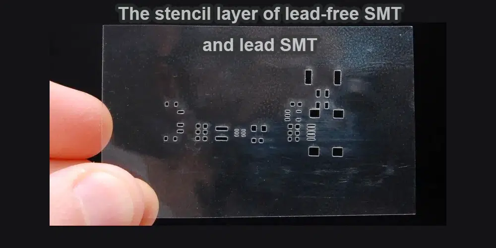
The design of the stencil layer still needs to consider the layout and application requirements of the solder paste, whether it is lead-free SMT or leaded SMT. The following are some subtle differences that may exist in the design of the stencil layer of lead-free SMT and lead SMT:
Formulation of Solder paste : The solder paste used for lead-free SMT usually does not contain lead, but other alloys are used instead of traditional leaded solder. Therefore, when designing the stencil layer, it may be necessary to use a stencil design that matches the lead-free solder paste formulation.
Temperature profile: The soldering temperature of lead-free SMT is usually higher than that of lead-based SMT because of the higher melting point of lead-free solder. The material and thickness of the stencil may need to be adjusted appropriately according to the soldering temperature profile to ensure that the solder paste is accurately applied at the correct temperature.
Package type: Due to the higher soldering temperature required by lead-free SMT, some special packages or components may not be suitable for lead-free SMT, but leaded SMT can only be used.
Therefore, when designing the stencil layer, it is necessary to determine the distribution and layout of the solder paste according to the package type and components used.
Overall, the design of stencil layer does not differ much between lead-free and leaded SMT. The main difference lies in aspects such as the solder paste formulation used and the soldering temperature profile. The stencil layer design still needs to be consistent with the PCB design file to ensure that the solder paste is properly applied to the pads of the surface mount components for reliable soldering. If lead-free SMT is used, it is also necessary to ensure that the solder paste and process used meet the requirements of lead-free soldering.
life span of stencil
Stencil is an important tool in the PCB assembly process, used to precisely apply solder paste in surface mount technology (SMT), and connect surface mount components (SMD) to the PCB. The number of uses of the stencil refers to how many times the stencil can be used in the assembly process within its useful life.
The usage count of the stencil is limited, mainly because of the gradual wear and fatigue during use. The following are factors that affect the number of times a stencil is used:
Thickness and Material: The thickness and material of the stencil will affect its durability and number of uses. Generally speaking, thicker stencils and stencils made of high-quality materials generally have a longer service life.
Quality: The quality and manufacturing process of the stencil are also important factors in determining the number of uses. High-quality stencils are more stable during use and can withstand more assembly cycles.
Assembly process: Some factors in the PCB assembly process, such as the characteristics of solder paste, soldering temperature and pressure, etc., will also affect the service life of the stencil.
Maintenance: Regular maintenance and cleaning of the stencil can extend its life. Remove solder paste residue and other dirt in a timely manner to ensure that the surface of the stencil remains smooth and flat.
Assembly scale: The service life of the stencil also depends on the scale of the assembly. Frequent use of stencils in mass production may result in faster wear.
Typically, the service life of a stencil is between a few thousand to tens of thousands of assembly cycles. Once the stencil has reached its upper limit of use or is severely worn, it needs to be replaced with a new stencil to ensure assembly quality and stability. Regular inspection and maintenance of stencil is a key measure to ensure its normal service life.

