With the rapid development of technology, the demand for signal transmission speed, bandwidth, and stability is becoming increasingly stringent, which has led to the emergence of high-frequency PCBs and microwave RF PCBs. High-frequency PCBs and microwave radio frequency (RF) PCBs both belong to the category of specialized printed circuit boards designed for handling high-frequency signals. Today, this article will delve into these two special types of PCBs, revealing their definitions, characteristics, differences, and intrinsic connections.
High-Frequency PCBs: the "Expressway" for High-Speed Signals
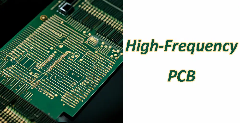
High-frequency PCBs, abbreviated as HF PCBs, refer to printed circuit boards specifically designed to handle signals with frequencies above 1GHz. These PCBs are mainly used to meet the requirements of modern electronic products for high-speed data transmission and high-frequency response, such as high-speed digital communication equipment, radar systems, satellite navigation equipment, etc.
Characteristics and Technical Points:
Material Selection: High-frequency PCBs typically use substrates with low dielectric constant (Dk) and low dielectric loss factor (Df), such as polytetrafluoroethylene (PTFE), ceramic-filled resin, etc., to reduce energy loss and delay during signal propagation.
Line Width/Spacing Control: To reduce crosstalk and signal distortion, high-frequency PCBs have strict requirements for wire width, spacing, and via size, requiring adherence to strict impedance control design rules.
Optimization of Layer Stackup: The multi-layer structure of high-frequency PCBs requires careful design. By adjusting the thickness, material, and position of each layer, the best impedance matching and signal integrity can be achieved.
Shielding and Grounding Design: To suppress electromagnetic interference (EMI), high-frequency PCBs often use embedded ground layers, shielding covers, or absorbing materials to enhance electromagnetic compatibility.
Microwave RF PCBs: Precision "Sound Engineers" for Wireless Signals
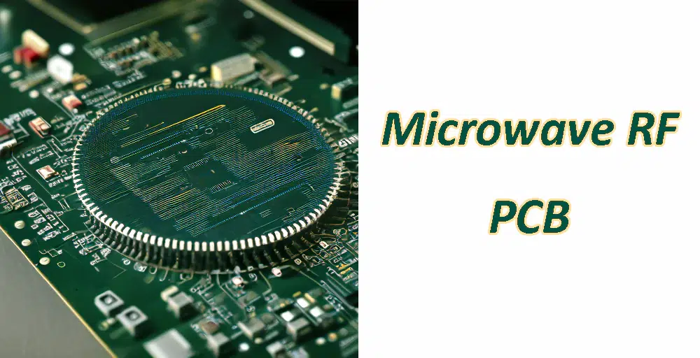
Microwave radio frequency PCBs, abbreviated as RF PCBs, are designed specifically to handle radio frequency (RF) signals in the microwave frequency range (typically from 300MHz to 300GHz). These PCBs are widely used in various fields such as wireless communication devices (e.g., smartphones, base stations), satellite communication, radar, and radio frequency identification (RFID) systems.
Characteristics and Technical Points:
High-Frequency Characteristics: As a special case of high-frequency PCBs, microwave RF PCBs also emphasize the selection of materials with low dielectric constant (Dk) and low dielectric loss factor (Df), as well as precise control of line width/spacing to ensure efficient transmission and precise tuning of RF signals.
Integration of RF Components: Microwave RF PCBs often need to accommodate various RF components (such as filters, amplifiers, mixers, etc.) and require sophisticated layout and routing to ensure impedance matching and signal transmission performance among these components.
Special Manufacturing Processes: Due to the sensitivity of RF signals, the manufacturing process of microwave RF PCBs may involve advanced techniques such as fine copper plating, laser drilling, buried vias, high-precision pattern transfer, etc., to ensure extremely high accuracy and consistency.
High-Frequency PCBs and Microwave RF PCBs
Similarities:
Fundamental Principles: Both are based on electromagnetic field theory and adhere to the same principles of signal integrity design, such as impedance control, reflection and crosstalk suppression, EMI protection, etc.
Materials and Processes: Both require the use of special substrates with low loss and low dispersion, and may involve advanced manufacturing processes to meet the demands of high-frequency signal transmission.
Differences
Operating Frequency Range:
Although both belong to the high-frequency domain, the operating frequency range of microwave RF PCBs is broader, covering a wide range from RF to microwave frequencies, with higher requirements for signal transmission stability and purity.
Application Fields:
High-frequency PCBs primarily serve high-speed digital communication equipment, focusing on fast and accurate data transmission. In contrast, microwave RF PCBs are focused on the processing and transmission/reception of RF signals in fields such as wireless communication and radar, emphasizing functions such as modulation, demodulation, filtering, etc.
Design Considerations:
High-Frequency PCBs: Focus on optimizing signal integrity, minimizing signal loss, and controlling impedance to ensure accurate and reliable high-speed data transmission. Design considerations include careful selection of materials with low dielectric constant and loss tangent, precise control of trace widths and spacing, and optimization of layer stackup.
Microwave RF PCBs: In addition to considerations for signal integrity, these PCBs also emphasize RF design principles such as impedance matching, minimizing radiation losses, and ensuring consistent RF performance across the operating frequency range. Design considerations may include integration of RF components, such as filters and amplifiers, and use of advanced manufacturing techniques to maintain signal integrity at higher frequencies.

