In the ever-evolving landscape of electronics, High-Density Interconnect (HDI) Printed Circuit Boards (PCBs) have emerged as a revolutionary technology, enabling compact, high-performance devices across various industries. Understanding the intricacies of HDI PCBs, from their construction to their applications, sheds light on their significance in modern electronics.
What is HDI PCB?
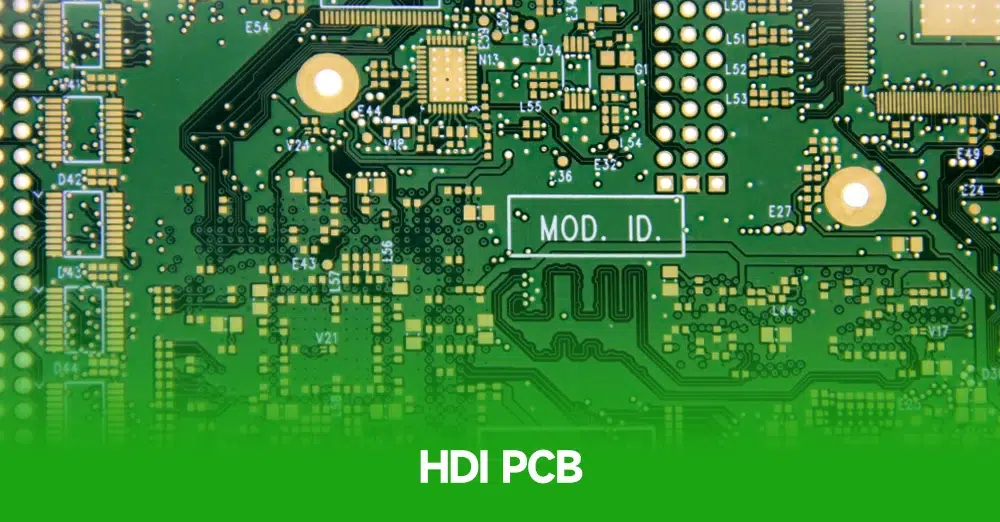
High-Density Interconnect PCBs, abbreviated as HDI PCBs, represent a class of circuit boards designed to maximize interconnection density. They achieve this by incorporating smaller vias, finer traces, and multiple layers of copper interconnects within a limited board space. HDI PCBs facilitate the integration of complex and dense circuitry, pushing the boundaries of miniaturization and functionality in electronic devices.
What is HDI Material?
The materials used in HDI PCBs play a critical role in their performance. Typically, HDI PCBs utilize advanced materials like high-performance laminates, specialized copper foils, and ultra-thin dielectrics. These materials offer enhanced electrical properties, increased signal integrity, and better thermal management, crucial for maintaining reliability in densely packed circuits.
What is HDI PCB Stack-up?
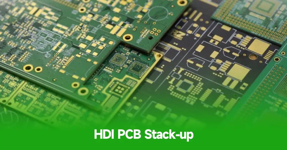
HDI PCB stack-up refers to the arrangement of layers within the circuit board. Unlike traditional PCBs, HDI stack-ups incorporate multiple layers of conductive traces and insulating substrates. The stack-up configuration varies based on the complexity of the design and the desired performance. HDI stack-ups often employ microvias, blind vias, and buried vias to interconnect different layers efficiently.
Lamination Process and Different Types of HDI PCB Stack-ups
The lamination process in HDI PCB manufacturing involves bonding multiple layers of substrates and copper traces using heat and pressure. Different types of HDI stack-ups include 1+N+1, 2+N+2, and 3+N+3, denoting the number of layers and the arrangement of buried and blind vias. These stack-ups allow for increased routing density and improved signal integrity in complex designs.
Differences Between HDI and Standard PCBs
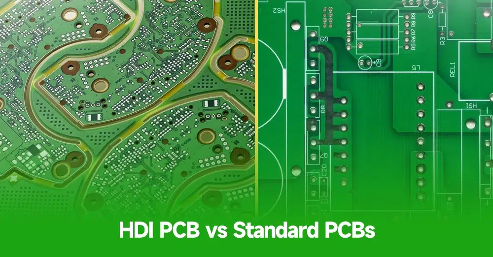
The primary distinctions between HDI and standard PCBs lie in their construction and capabilities. HDI PCBs offer higher interconnect densities, finer traces, and smaller vias compared to traditional PCBs. This enables them to accommodate more components and complex circuits in a smaller footprint, enhancing performance and functionality.
Benefits of HDI PCB
The advantages of HDI PCBs are manifold:
Miniaturization: HDI technology allows for smaller, lighter, and more compact electronic devices.
Enhanced Performance: Improved signal integrity, reduced signal loss, and better thermal management contribute to superior performance.
Increased Reliability: With minimized interference and optimized power distribution, HDI PCBs exhibit higher reliability.
Cost Efficiency: Despite their complexity, HDI PCBs can reduce overall system costs by eliminating the need for additional components and layers.
Applications of HDI PCB
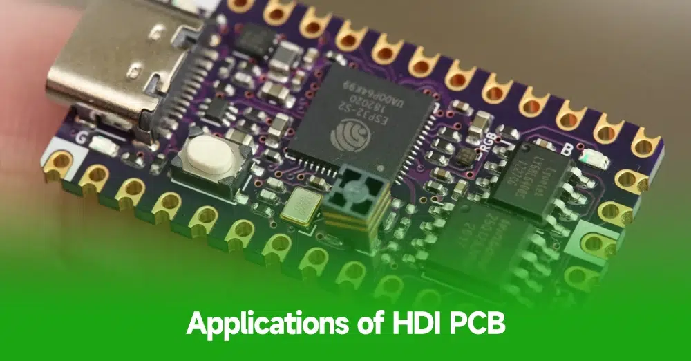
HDI PCBs find extensive applications in various industries:
Consumer Electronics: Smartphones, tablets, wearables, and compact computing devices benefit from HDI PCBs’ miniaturization capabilities.
Telecommunications: High-speed data transmission equipment, networking devices, and satellite systems leverage HDI PCBs for their high-density interconnects.
Medical Devices: Medical imaging equipment, implantable devices, and diagnostic tools utilize HDI PCBs for their reliability and compact design.
Design and Manufacturing Processes of HDI PCB
The design process of HDI PCBs involves intricate planning of layer stack-ups, placement of components, and routing of traces using specialized software. Manufacturing involves precision drilling of microvias, copper plating, lamination of layers, and surface finishing to achieve the desired electrical and mechanical properties.
In conclusion, HDI PCBs stand at the forefront of technological innovation, enabling smaller, faster, and more efficient electronic devices across diverse industries. Their advanced materials, intricate stack-ups, and superior performance characteristics continue to drive progress in the ever-evolving world of electronics. As demands for miniaturization and functionality persist, the role of HDI PCBs remains pivotal in shaping the future of electronic design and manufacturing.
High-Density Interconnect PCBs, abbreviated as HDI PCBs, represent a class of circuit boards designed to maximize interconnection density. They achieve this by incorporating smaller vias, finer traces, and multiple layers of copper interconnects within a limited board space. HDI PCBs facilitate the integration of complex and dense circuitry, pushing the boundaries of miniaturization and functionality in electronic devices.
The materials used in HDI PCBs play a critical role in their performance. Typically, HDI PCBs utilize advanced materials like high-performance laminates, specialized copper foils, and ultra-thin dielectrics. These materials offer enhanced electrical properties, increased signal integrity, and better thermal management, crucial for maintaining reliability in densely packed circuits.
HDI PCB stack-up refers to the arrangement of layers within the circuit board. Unlike traditional PCBs, HDI stack-ups incorporate multiple layers of conductive traces and insulating substrates. The stack-up configuration varies based on the complexity of the design and the desired performance. HDI stack-ups often employ microvias, blind vias, and buried vias to interconnect different layers efficiently.

