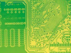
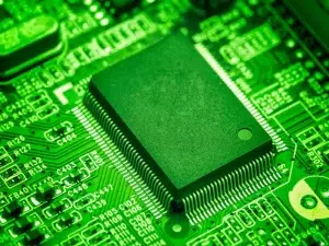
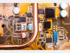
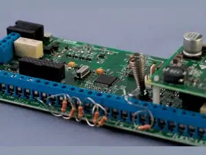
A high-frequency PCB is designed to efficiently transmit high-frequency signals for electronics operating above 3 GHz.
As faster data rates drive signal frequencies higher across wireless, satellite, defense and communication applications, PCBs must facilitate reliable routing of increasingly higher frequencies.
What is a High-Frequency PCB?
A high-frequency PCB is engineered to carry signals with frequencies typically above 3 GHz (microwave range), minimizing losses during transmission. High speed signals require matched impedance traces, precise dielectric constants, and specialized materials to maintain signal integrity as frequencies rise into millimeter wave and beyond.
What are the Features of High-Frequency PCBs?
High-frequency PCB requires specialized design elements and materials to effectively carry signals above 3 GHz without excessive loss or interference:
Controlled Impedance Traces – Carefully tuned trace width, thickness, and dielectric match the impedance for efficient power transfer without reflections.
Layered Dielectrics – Thin, uniform dielectric layers using low-loss substrates reduce signal loss and propagation delay while smoothing layers reduces surface roughness that scatters high-frequency signals.
Fine Line Geometries – Narrow trace widths and spacing paired with smaller vias enables higher component density essential for reducing path lengths in order to maintain signal integrity at microwave/mmWave frequencies.
Ground and Power Planes – Continuous reference planes shield signals from noise interference and crosstalk which increases at higher frequencies due to faster rise times. Decoupling capacitors filter noise between planes.
Smooth Copper and Dielectrics – Surface roughness scatters signals, thereby losing power so smooth, flat copper and dielectrics are vital for reducing skin effect losses as frequencies increase into the GHz bandwidth.
Together these PCB enhancements concentrate on precision impedance control, shielding, tightened component spacing, smoothed materials, and low-loss dielectrics to counter signal degradation challenges prominent at high operating frequencies.
What’s the applications of High-Frequency PCBs?
As data and bandwidth demands escalate across electronics ecosystems, high-frequency PCB technology provides connectivity foundations across cutting-edge microwave and mmWave systems:
• Aerospace and Defense – Radar arrays, electronic warfare, satellite payloads, and communications infrastructure operate in X, Ku and Ka frequency bands, relying on PCBs handling 10+ GHz signals with minimal loss.
• Wireless Infrastructure – Microwave backhaul links and emerging 5G networks employ mmWave signals above 24 GHz between base stations, dependent on HF circuit boards.
• High-Speed Testing – Oscilloscopes, electronic test and measurement systems require HF PCBs to acquire signal data, synthesize waveforms and process information.
• Medical Imaging – MRI, PET and CT scanners as well as laser surgery equipment integrate control, monitoring and power delivery electronics with HF boards.
• Autonomous Technology – Sensor data fusion in self-driving vehicles and drones, demands extreme data rates and bandwidth connecting LIDAR, cameras, radar and more via HF PCB links.
The need for speed and bandwidth connects advanced capability across crucial strategic high-frequency electronics, with HF PCB innovation delivering the foundation.
What materials are used for High-Frequency PCBs?
High-frequency PCB fabrication utilizes low-loss substrates with stable electrical and thermal properties to maintain signal integrity without excessive material-related attenuation or distortion above 3 GHz:
• PTFE Composites – Woven fiberglass reinforced polytetrafluoroethylene (PTFE) composites like Rogers RO3000 series combine the low dielectric loss of pure PTFE with reduced coefficient of thermal expansion for dimensional stability.
• Ceramic Filled PTFE – Ceramic particles blended with PTFE matrices create microelectronics-grade substrates with reduced permeability and moisture absorption compared to conventional glass fabric composites alone.
• Hydrocarbon Resins – Polyimides, cyanate esters, and liquid crystal polymers offer lowered dielectric loss tangents below 0.005, critical for minimizing signal losses at microwave frequencies.
• Glass Fabric Dielectrics – Tightly controlled woven fiberglass with resin bonding gives mechanical support while strongly adhering thin laminates onto plane layers with highly consistent thickness across HF PCBs.
Precise combinations of resin systems, reinforcement fabrics, fillers and fiber weaves allow specialized materials science to create advanced substrates balancing electrical, thermal, and mechanical needs for raising PCB operating frequencies past legacy limits.
Which transistor is most suitable for high-frequency circuits
As circuits approach microwave and millimeter-wave frequencies, silicon bipolar junction transistors (BJTs) encounter unity gain cut-off limits around 200 GHz, requiring alternative solid-state devices optimized for ultra high-speed operation.
Gallium Arsenide (GaAs) Heterojunction Bipolar Transistors (HBTs) integrate gallium arsenide and aluminum gallium arsenide layers, taking advantage of bandgap engineering and electron mobility improvements to reach unity gain cut-off frequencies over 250 GHz. This enables power gain and amplification supporting mmWave radio designs exceeding 90 GHz.
GaAs HBTs also provide high breakdown voltages and current density capabilities relative to size. This permits handling of the increased power levels needed to transmit signals at very high frequencies. Parasitic capacitance and inductance is also reduced by smaller feature geometries.
With silicon BJTs hitting speed limits around 200 GHz, GaAs HBT innovation empowers next generation microwave and mmWave systems pushing signal frequencies ever higher through transistor advancements synergizing material science with electronic design.
How to design a high-frequency PCB?
Successfully transmitting signals above 3 GHz demands precision design techniques to prevent excessive losses or impedance mismatches during high-speed propagation:
1. Electromagnetic Simulation – 3D EM modeling software like Ansys HFSS simulates circuit performance, visualizing effects from component placement to trace geometries in order to optimize the layout.
2. Controlled Impedance Modeling – Tools extract parasitic values from geometry, materials and layer stackups, generating accurate transmission line models to match trace impedance for efficient power transfer.
3. Topology Optimization – Algorithms determine optimal component layouts and trace routing to minimize path lengths and abrupt directional changes during signal traversal while meeting tight mechanical constraints.
4. Thermal Modeling – Simulation contrasting operating power and heat sink effectiveness ensures temperature profiles won’t diminish electrical performance or exceed material limits.
These modeling capabilities transform higher frequency needs like impedance control, adequate shielding and thermal stability into actionable, optimized PCB design rule sets.
What's the fabrication process for high-frequency PCBs?
The fabrication process for high-frequency printed circuit boards (PCBs) involves several specialized steps to ensure optimal performance at higher frequencies. High-frequency PCBs are designed to handle signals in the radio frequency (RF) and microwave ranges, where signal integrity and minimal signal loss are critical. Here is an overview of the key steps in the fabrication process for high-frequency PCBs:
1. Material Selection:
Choose a high-performance substrate material with low dielectric constant (Dk) and low dissipation factor (Df) to minimize signal loss and maintain signal integrity. Common high-frequency substrate materials include PTFE (Teflon), RO4003, RO4350, and polyimide.
2. Prepreg Selection:
Prepregs are layers of material impregnated with resin that are used to bond the layers of the PCB together. Select prepregs with characteristics that match the chosen substrate material to maintain consistency in electrical properties.
3. Layer Stackup Design:
Design the layer stackup to meet the impedance requirements and control the characteristic impedance of transmission lines. High-frequency PCBs often use controlled impedance structures to minimize signal distortion.
4. Copper Foil Lamination:
Laminate the layers of the PCB stackup using heat and pressure. Ensure proper alignment and bonding of the copper layers and prepregs. This step is critical for maintaining consistent electrical performance.
5. Drilling:
Precision drilling is performed to create holes for vias and component mounting. High-frequency PCBs may require smaller drill sizes and tighter tolerances to maintain signal integrity.
6. Copper Plating:
Deposit a thin layer of copper onto the drilled holes to create vias. This step is crucial for creating a conductive path between different layers of the PCB.
7. Circuit Pattern Imaging:
Use a photolithography process to transfer the PCB circuit pattern onto the substrate. This involves applying a photoresist, exposing it to UV light through a photomask, and then developing the pattern.
8. Etching:
Etch away the unwanted copper using chemical processes, leaving behind the desired circuit traces. Precision etching is essential to maintain the accuracy of the circuit dimensions.
9. Surface Finish:
Apply a suitable surface finish to protect the exposed copper and enhance solderability. Common surface finishes for high-frequency PCBs include immersion gold, immersion silver, or immersion tin.
10. Solder Mask Application:
Apply a solder mask to protect the PCB surface and define areas for soldering components. The solder mask also contributes to electrical insulation.
11. Component Assembly:
Mount and solder components onto the PCB following industry-standard assembly processes. Ensure that the assembly techniques are compatible with high-frequency applications.
12. Testing:
Perform electrical testing, including impedance testing and high-frequency testing, to verify that the fabricated PCB meets the specified requirements for signal integrity and performance.
Considerations when Choosing High-Frequency PCB Substrates
Electrical and thermal properties must be balanced when selecting high-frequency PCB substrates. Key factors include dielectric constant, loss tangent, thermal conductivity and the coefficient of thermal expansion.
Choosing the right high-frequency PCB substrate is crucial for achieving optimal performance in applications involving radio frequency (RF) and microwave signals. Several considerations should be taken into account when selecting high-frequency PCB substrates:
Dielectric Constant (Dk):
The dielectric constant, often denoted as Dk, is a key parameter determining the speed of signal propagation through the substrate material. Lower Dk values are generally preferred for minimizing signal delay and maintaining signal integrity.
Dielectric Loss (Df):
Dielectric loss, or dissipation factor (Df), represents the energy lost as heat during signal transmission. Lower Df values are essential for reducing signal loss and achieving higher efficiency in high-frequency applications.
Copper Clad Thickness:
The thickness of the copper layer on the substrate affects the impedance characteristics of the PCB. Thinner copper layers can contribute to lower losses, but they may also have higher resistance. The choice depends on the specific requirements of the application.
Substrate Material:
Common high-frequency substrate materials include polytetrafluoroethylene (PTFE or Teflon), ceramic-filled PTFE, and hydrocarbon ceramic laminates. Each material has its advantages and disadvantages in terms of cost, performance, and manufacturability.
Thermal Stability:
High-frequency PCBs may experience temperature variations during operation. Choosing a substrate material with good thermal stability ensures that the electrical properties remain consistent over a range of temperatures.
Frequency Range:
Different applications may have specific frequency requirements. Ensure that the selected substrate material is suitable for the intended frequency range of the application.
Conclusion
As electronics push into the Era of Terahertz, high-frequency PCB innovations will continue powering complex microwave and millimeter-wave systems underlying leading-edge wireless infrastructure, radars for autonomous platforms, satellites transmitting massive data loads, and beyond.
Advancements in high-frequency PCB materials and precision modeling and fabrication will synergize growing high-speed demands with capabilities to maintain signal integrity.
With communication systems evolving toward higher-frequency bands above 90 GHz and eventually 300 GHz to leverage new bandwidth capacity, the key role of the underlying high-frequency PCB technology often goes unseen despite enabling these cutting-edge innovations through electrical engineering disciplines.
A high-frequency PCB is engineered to carry signals with frequencies typically above 3 GHz (microwave range), minimizing losses during transmission.
Aerospace and Defense
Wireless Infrastructure
High-Speed Testing
Medical Imaging
Autonomous Technology
PTFE Composites
Ceramic Filled PTFE
Hydrocarbon Resins
Glass Fabric Dielectrics

