Integrated circuits (ICs) have been the backbone of modern electronics, enabling the creation of powerful and compact electronic devices. At the heart of these ICs lies a crucial element that often goes unnoticed – the integrated circuit packages. These packages play a vital role in protecting and enhancing the performance of ICs, allowing them to thrive in diverse applications ranging from smartphones and computers to medical devices and automotive systems.
The Basics of Integrated Circuit Packages
An integrated circuit packages serve as a protective and functional housing for the delicate semiconductor die within. It provides mechanical support, electrical connections, and thermal management to ensure the reliable operation of the integrated circuit. These packages come in various shapes and sizes, tailored to specific applications and requirements.
Types of Integrated Circuit Packages
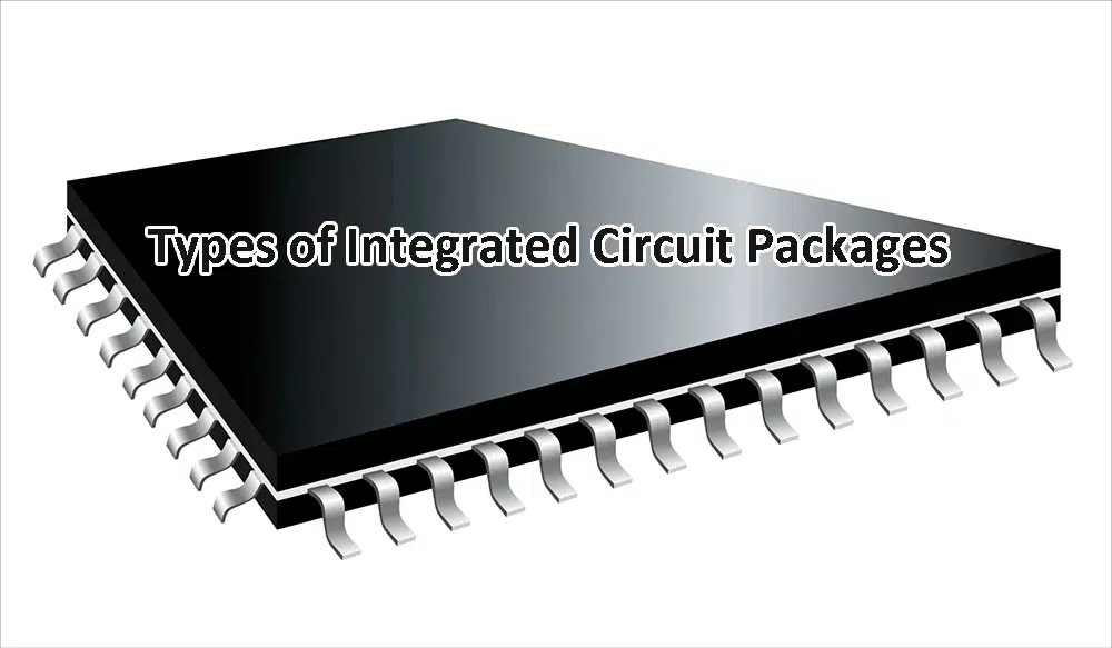
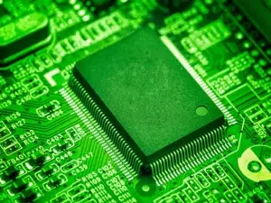
Quad Flat Package (QFP): QFP features a square or rectangular body with pins extending from all four sides. It provides a higher pin density compared to DIP, making it suitable for applications where space is a critical factor.
Ball Grid Array (BGA): In BGA packages, solder balls replace traditional pins, allowing for more compact designs. BGAs are commonly used in applications requiring high-density connections and are prevalent in consumer electronics, such as laptops and gaming consoles.
Chip-on-Board (COB): In COB packaging, the semiconductor die is directly mounted onto the circuit board, eliminating the traditional package. This minimizes size and enhances thermal performance, making it suitable for space-constrained applications.
System-in-Package (SiP): SiP takes integration to the next level by combining multiple ICs, passive components, and sometimes even MEMS (Micro-Electro-Mechanical Systems) into a single package. This approach enhances performance, reduces power consumption, and optimizes space utilization.
How are integrated circuits packaged?
The process of packaging integrated circuits involves the following steps:
1. Die Attachment: The semiconductor die (the actual integrated circuit) is attached to a lead frame or a substrate within the package. This is typically done using adhesive materials.
2. Wire Bonding: Thin wires (usually made of aluminum or gold) are used to establish electrical connections between the die and the lead frame or substrate. This process is known as wire bonding.
3. Encapsulation: The die and wire bonds are encapsulated in a protective material, often epoxy resin or plastic, to shield them from environmental factors and physical damage. The encapsulation also provides mechanical strength to the package.
4. Molding: The encapsulated assembly is placed in a mold, and a molding compound is injected to form the final package shape. This molding process helps in creating a uniform and protective outer shell for the IC.
5. Lead Formation: If a lead frame is used, the leads (metal legs) are formed into the desired shape for external connections. In surface-mount packages, the leads may be absent, and instead, solder pads or balls are used for mounting on a printed circuit board (PCB).
6. Marking and Testing: The packaged ICs are marked with identification codes, logos, and other information for traceability. They are then subjected to various electrical tests to ensure they meet the specified performance criteria.
Advancements in Integrated Circuit Packages
The evolution of integrated circuit packages has been driven by the constant demand for smaller, faster, and more efficient electronic devices. Advanced packaging technologies include:
Flip-Chip Technology: In this method, the IC is flipped upside down, and solder bumps connect the die directly to the substrate, improving thermal performance and signal integrity.
3D IC Packaging: Stacking multiple ICs on top of each other allows for increased functionality in a smaller footprint. This approach enhances performance by reducing interconnect lengths and improving data transfer rates.
Wafer-Level Packaging (WLP): WLP involves packaging multiple ICs simultaneously on the wafer before they are separated. This improves cost efficiency and allows for more compact designs.

Conclusion
Integrated circuit packages are integral components that enable the miniaturization and functionality of modern electronic devices. As technology continues to advance, the development of innovative packaging solutions will play a crucial role in meeting the ever-growing demands for smaller, more powerful, and energy-efficient electronics. The intricate world of integrated circuit packages underscores the importance of marrying form and function to drive the digital age forward.

