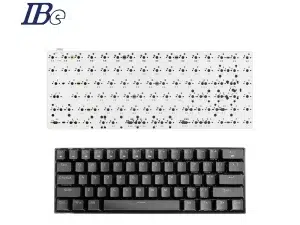
Printed Circuit Boards (PCBs) are the backbone of almost all modern electronic devices, from smartphones and computers to medical equipment and automotive systems. The process of creating a PCB involves several steps, one of the most crucial being the creation of the PCB artwork. In this article, we will delve into what PCB artwork is, how it is created, its importance, and its role in the overall PCB design and manufacturing process.
What is PCB Artwork?
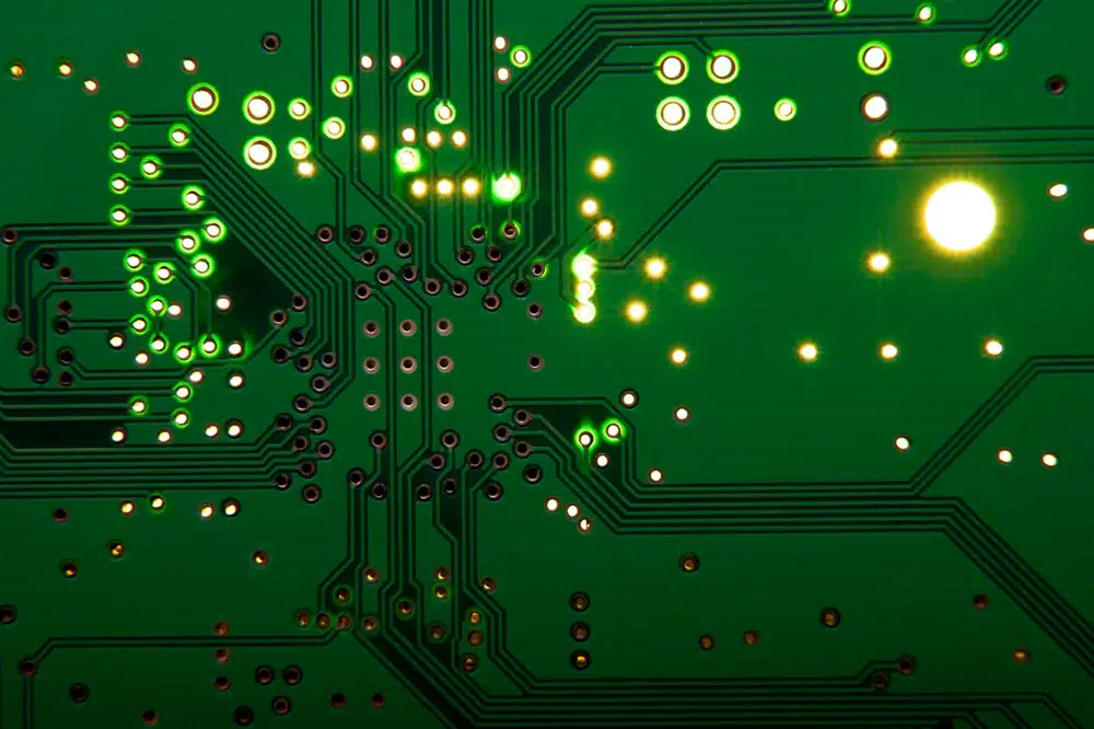
PCB artwork refers to the visual representation or layout of the electrical components and conductive traces on a printed circuit board. It is essentially a schematic design that guides the manufacturing process of the PCB. This design includes the arrangement of components, the paths for electrical signals, and the layers of the board. PCB artwork is usually created using specialized design software that converts the engineer’s or designer’s schematic into a form that can be transferred to the PCB substrate during manufacturing.
In its simplest form, PCB artwork consists of:
– Traces: The copper paths that connect different components on the PCB.
– Pads: The locations where electronic components are soldered onto the board.
– Vias: Small holes that connect different layers of the PCB, used in multi-layer designs.
– Silkscreen Layer: This contains labels, component outlines, and other marks to help in component placement and assembly.
– Ground and Power Planes: Layers that provide stable power and grounding to components.
What is PCB Artwork used for?
The artwork is the blueprint for the PCB. It provides a detailed layout that ensures the proper electrical connections and mechanical design of the board. Poor or incorrect PCB artwork can result in several issues such as:
– Electrical Failures: Incorrect trace widths or inadequate grounding can lead to poor performance or even complete failure of the circuit.
– Manufacturing Defects: If the design is not properly translated to the physical board, it can cause defects during manufacturing, resulting in non-functional or defective PCBs.
– Difficulty in Assembly: Improper placement of components or unclear silkscreen markings can complicate assembly, leading to longer production times or increased error rates.
– Signal Integrity Issues: Trace routing and component placement can significantly affect signal integrity, especially in high-frequency designs. Poor PCB artwork can cause issues like noise or cross-talk between signals.
Given its critical role, the creation of PCB artwork is one of the most important steps in the PCB design process. It requires careful attention to both electrical and mechanical aspects of the design.
How is PCB Artwork Created?
Creating PCB artwork involves several stages, from the initial schematic design to the final physical layout that can be sent to the manufacturer. The following steps outline the typical process:
1. Schematic Design
Before PCB artwork can be created, a schematic diagram of the circuit is made. The schematic is a logical representation of how the components are connected and how signals flow between them. It doesn’t consider physical layout, but it is the starting point for the PCB design. The schematic will include all components, such as resistors, capacitors, ICs, and connectors, along with their electrical connections.
2. Component Placement
Once the schematic is completed and validated, the next step is to place the components on the PCB layout. During this phase, engineers or designers determine where each component will go on the PCB surface. This placement is done with consideration of:
– Electrical considerations: Placing components close together to minimize trace lengths and reduce noise.
– Thermal management: Ensuring heat-sensitive components are placed appropriately to avoid overheating.
– Mechanical constraints: Avoiding interference with connectors, mounting holes, or the PCB edge.
Component placement is a delicate balance between optimizing electrical performance and meeting manufacturing constraints, as well as considering future assembly and maintenance needs.
3. Routing and Trace Design
Once components are placed, the next step is to connect them with copper traces. The routing process involves drawing the electrical traces that will physically connect the pads of each component. There are several factors that need to be considered during this stage:
– Trace Width: The width of the copper traces determines the amount of current they can safely carry. Wider traces are used for higher currents, while narrower traces are used for signals or low-power connections.
– Trace Spacing: Proper spacing between traces is essential to avoid short circuits or signal interference.
– Layering: Multi-layer PCBs have additional layers for routing signals and power/ground planes. Vias are used to connect traces between layers.
The routing stage is one of the most complex parts of the PCB artwork creation process, particularly for high-density and high-speed designs.
4. Design Rule Check (DRC)
After the artwork is created, a Design Rule Check (DRC) is performed to ensure the design adheres to the manufacturer’s requirements and industry standards. DRC ensures that the traces are wide enough to handle the intended current, that the spacing is sufficient to prevent shorts, and that vias are placed correctly. This step is critical to ensure the PCB can be manufactured without defects.
5. Generating Gerber Files
Once the design has passed all checks, it is converted into Gerber files. Gerber files are the standard file format used by PCB manufacturers to produce the physical board. These files contain all the necessary information for manufacturing the PCB, including:
– Copper layers
– Drill holes for vias and component leads
– Solder mask layers (used to protect the copper traces)
– Silkscreen layer (used for labeling component positions and other markings)
6. Bill of Materials (BoM)
Along with the Gerber files, a Bill of Materials (BoM) is generated. This is a list of all components that will be used in the assembly of the PCB. The BoM includes component values, part numbers, and quantities, helping the assembly team source and organize components.
What are the Tools for PCB Artwork Creation?
Various PCB design software tools are used to create PCB artwork. Some of the most popular ones include:
– Altium Designer: A comprehensive design suite that supports schematic capture, PCB layout, and DRC. It is widely used in both professional and industrial design.
– KiCad: An open-source PCB design tool that includes schematic capture and PCB layout capabilities.
– Autodesk Eagle: A popular tool for hobbyists and professionals alike, offering a range of features for PCB design.
– OrCAD: A professional PCB design software often used in complex designs requiring high-level functionality.
These tools help automate many aspects of the PCB design process, from trace routing to error checking, making it easier for designers to create high-quality, manufacturable PCB artwork.
What’s the Role of PCB Artwork in the Manufacturing Process?
PCB artwork serves as the direct blueprint for manufacturing the PCB. Once the Gerber files are sent to the PCB manufacturer, the physical board is fabricated using processes such as photolithography, etching, and solder mask application. The accuracy of the artwork is directly linked to the quality of the final product. Inaccuracies or mistakes in the artwork can result in production delays, additional costs, or functional failures in the final product.
Conclusion
PCB artwork is a fundamental aspect of PCB design and manufacturing. It defines the physical layout and electrical connections of the circuit board, providing the crucial blueprint that guides the creation of the final product. A well-designed PCB artwork ensures reliable electrical performance, manufacturability, and ease of assembly, while a poorly designed one can lead to costly errors, delays, and product failures.
As technology continues to evolve, the importance of high-quality PCB artwork will only increase. Engineers and designers must leverage the latest tools and design methodologies to create PCBs that meet the ever-growing demands for performance, miniaturization, and cost-effectiveness. Whether you are working on a simple hobby project or a complex industrial application, understanding the intricacies of PCB artwork is essential for creating successful electronic products.
PCB artwork refers to the visual representation or layout of the electrical components and conductive traces on a printed circuit board. It is essentially a schematic design that guides the manufacturing process of the PCB.
Various PCB design software tools are used to create PCB artwork. Some of the most popular ones include:
- Altium Designer: A comprehensive design suite that supports schematic capture, PCB layout, and DRC. It is widely used in both professional and industrial design.
- KiCad: An open-source PCB design tool that includes schematic capture and PCB layout capabilities.
- Autodesk Eagle: A popular tool for hobbyists and professionals alike, offering a range of features for PCB design.
- OrCAD: A professional PCB design software often used in complex designs requiring high-level functionality.
The artwork is the blueprint for the PCB. It provides a detailed layout that ensures the proper electrical connections and mechanical design of the board. Poor or incorrect PCB artwork can result in several issues such as:
- Electrical Failures: Incorrect trace widths or inadequate grounding can lead to poor performance or even complete failure of the circuit.

