For any printed circuit board to be successfully manufactured, critical design data must be accurately translated from the schematic and layout design files into a format ready for the PCB fabrication process.
This special file type containing all relevant layer by layer graphical content is known as the PCB Gerber file. As the standard interface file between PCB designers and manufacturers, getting the Gerber output correct is essential.
This article serves to explain the key components of a Gerber file, how they are created from design tools, common viewing techniques and factors making the RS-274X format an industry standard.
With a clear understanding of Gerber, designers can efficiently provide fab facilities with complete data to reproduce boards true to the envisioned concept.
What Files are Required for PCB Manufacturing?
When manufacturing a printed circuit board, there are a few key file types that are required to be submitted to a PCB fabrication factory.
The most important of these is the Gerber file. Other common file types include the Schematic file, Assembly Drawing file and Bill of Materials.
What is a PCB Gerber file?
A PCB Gerber file contains the graphical design data for each layer of the PCB design.
It provides a visual representation of where copper traces, components and other design elements need to be placed on each individual layer of the printed circuit board.
Common layers that will have their own Gerber file include the top copper layer, bottom copper layer, soldermask layers, legend text and drill drawing.
Why is Gerber file important in PCB manufacturing?

These phototools are then used in the manufacturing process to expose different materials like copper clad and remove copper from unwanted areas, forming the required PCB patterns.
Without an accurate PCB Gerber file, the manufacturer would not be able to produce the board according to the original design intent.
How many layers does a Gerber file have?
A typical PCB Gerber file set contains individual files for each layer of the PCB design. Common layers include soldermask, legends, top and bottom copper pours.
More complex multilayer PCBs may contain inner copper layers, Assembly Keepout areas and others. Most designs will require separate Gerber files for at least 4-5 layers.
What is the difference between Gerber and a schematic file?
A schematic shows the circuit connectivity and component relationships using graphical symbols.
On the other hand, a PCB Gerber file depicts the physical printed circuit board with accurate dimensions, outlines and individual copper traces/pads for each layer.
Schematics are used early in the design process, while Gerber files are needed later for manufacturing.
How do I create a Gerber file?
Design the schematic circuit using EDA software
First, use a program like Altium Designer, KiCad or Eagle to draw out the circuit schematic diagram. Specify component designators, pin connections etc.
Create PCB board layout
Take the schematic netlist and begin laying out the printed circuit board layers in the EDA software. Place components, draw PCB tracks, pour copper areas.
Setup design layers
Configure the required board layers like Top Copper, Bottom Copper, Soldermask etc. Assign net classes and design rules.
Run DRC and generate fabrication outputs
Perform a design rules check to validate PCB manufacturability. Then generate outputs needed for fabrication like ODB++, NC Drill and Gerber files.
Export Gerber files
From the EDA software, navigate to the output generation tools. Select the Gerber file format (RS-274X typically) and generate individual Gerber files for each PCB design layer.
Inspect Gerber outputs
Use a Gerber viewer to inspect each exported layer file and check contents that match the PCB layout. Make modifications if needed before submitting files.
Submit job to fabricator
Package all necessary files like Gerber set, BOM, assembly drawing etc and submit the job package to your selected PCB fabrication factory for manufacturing.
By following these steps in EDA software and carefully exporting and inspecting Gerber files, designers can ensure accurate data is delivered to the PCB manufacturer for high quality production.
How do I view Gerber files?
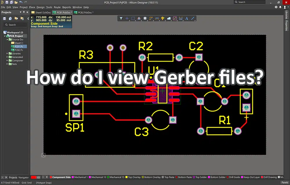
Popular free and paid viewers include GSK Citrix Viewer, Polar Viewer, and ViewMate. Download and install the desired viewer onto your computer.
Open Gerber files
Launch the viewer program and select “Open” then locate and open each individual Gerber file (.gbr, .gko etc) for the project.
Set up view parameters
Configure settings like units of measurement, scale factor, colors etc as needed for clear viewing of layers.
Navigate between layers
Use layer selection tabs or drop down menus to toggle between all Gerber files opened, viewing one at a time.
Adjust view window
Pan and zoom inside the viewing window using tools or mouse to focus on details across the board area.
Inspect layer graphics & info
Visually examine graphics, apertures and position data on each PCB layer for accuracy against design intent.
Validate aperture sizes
You can retrieve numeric aperture sizes from the Gerber file and cross-check drill hole sizes for example.
Compare revision files
If viewing two design revisions, select overlay mode to see differences using layer visibility and color coding tools.
Save screenshots
Use built-in screenshot capture functions to save images of any layers needing approval or rework.
Troubleshoot problem files
Viewersoftwares provide error logs that can aid debugging poorly formatted or erroneous Gerber files.
Taking time to thoroughly view outputs helps vet Gerber data before proceeding to fabrication.
What is the commonly used Gerber format?
The most widespread Gerber format adopted across the PCB design and fabrication industry is known as RS-274X. Here are some more details about this standard:
Specification – RS-274X is formally specified by the Association Connecting Electronics Industries (IPC). It defines the file structure, coordinate systems, commands and aperture/graphic elements.
Open Standard – As an open standard, the specification documentation is freely available which has helped drive its widespread adoption. Proprietary formats lack this openness.
File Extension – Files conforming to RS-274X use the .gbr or occasionally .gml file extensions to indicate the format.
Components – Data is organized into header records describing boards/layers. Aperture records describe graphic elements like circles/polygons. Draw records contain coordinate plotting commands.
Coordinate Systems – Both absolute (ICHIP) and incremental (IPOS) positioning can be used, with origin placement in the lower-left corner by convention.
Supported Elements – Elements like vector draws, circular copper pads and SMD pads can all be represented along with attributes like width, drill size etc.
Viewer Compatibility – Virtually all commercial Gerber viewers natively support RS-274X ensuring cross-platform compatibility for exchanging design data.
Adoption drivers – The open standard simplifies data exchange across tools and geographic regions. Its maturity resulted from being around since the 1980s and addressing most use cases over the years.
While some legacy or specialized use cases may utilize other formats, RS-274X has become the de facto standard that the vast majority of modern PCB designers and manufacturers rely on for new projects due to its widespread acceptance and ongoing support within the industry.
Conclusion
In conclusion, the PCB Gerber file contains vital graphical design data at a layer level needed by PCB fabricators.
Designers must supply accurate Gerber outputs to guarantee their envisioned designs are produced correctly.
Understanding key aspects like typical layers, manufacturing usage and creation process enables efficient Gerber based communication with manufacturers.
A PCB Gerber file contains the graphical design data for each layer of the PCB design.
It provides a visual representation of where copper traces, components and other design elements need to be placed on each individual layer of the printed circuit board.
A typical PCB Gerber file set contains individual files for each layer of the PCB design. Common layers include soldermask, legends, top and bottom copper pours.
A schematic shows the circuit connectivity and component relationships using graphical symbols.
On the other hand, a PCB Gerber file depicts the physical printed circuit board with accurate dimensions, outlines and individual copper traces/pads for each layer.


