In the fast-evolving realm of electronics, where devices are becoming more compact yet increasingly complex, the demand for flexible and adaptable circuitry is paramount. Rigid flex PCB emerges as a transformative solution, seamlessly blending the robustness of rigid boards with the flexibility of flexible circuits. This amalgamation propels a new era in electronics design, enabling innovations that transcend traditional limitations.
Flex rigid PCBs find applications in various industries, including aerospace, automotive, medical devices, and consumer electronics, where their ability to accommodate complex designs, reduce space, and enhance reliability is advantageous.
What is flex rigid PCB?
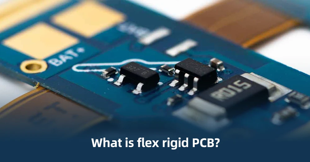
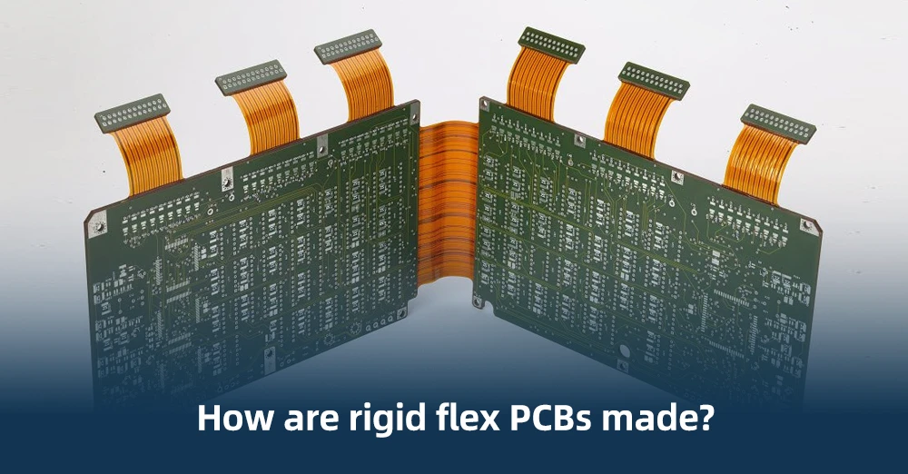
Flex rigid PCBs are a type of printed circuit board (PCB) that combines both flexible and rigid board technologies within a single design. They offer the advantages of both flexible and rigid PCBs, allowing for complex three-dimensional configurations while maintaining structural stability and durability.
These boards consist of flexible circuit substrates joined with rigid boards using plated through-holes or other connection methods. The flexible portions enable bending or folding, making them suitable for applications requiring intricate shapes or where space is limited. Meanwhile, the rigid sections provide support and stability for components that require a solid mounting surface.
What are the advantages and disadvantages of rigid flex PCB?
Rigid flex PCB offers a blend of advantages from both rigid and flexible PCBs, but they also come with some specific considerations:
Advantages:
Space Saving: Rigid flex PCB designs reduce the need for connectors and wiring, saving space in compact devices where size is crucial.
Reliability: Fewer solder joints and connectors decrease the risk of failure due to loose connections or wire fatigue, enhancing overall reliability.
Complex Designs: They allow for intricate three-dimensional configurations and can fit into unconventional shapes or limited spaces, offering design flexibility.
Weight Reduction: By eliminating the need for additional wiring and connectors, they can contribute to weight reduction in devices or systems.
Improved Signal Integrity: Reduced electromagnetic interference and signal loss due to shorter signal paths and better impedance control.
Disadvantages:
Complex Manufacturing: Rigid flex PCBs are more complex to manufacture compared to standard rigid or flexible PCBs, which can increase production costs.
Design Challenges: Designing rigid flex PCB requires specialized expertise and tools. Changes in design mid-production can be expensive and time-consuming.
Testing and Repair: Testing and repairing rigid flex PCB can be more challenging due to their complex structure and interconnections.
Higher Cost: Their specialized manufacturing process, materials, and the complexity of design contribute to higher costs compared to traditional PCBs.
Limited Suppliers: Not all PCB manufacturers offer rigid flex capabilities, limiting options and potentially leading to longer lead times or higher costs.
Despite these considerations, the advantages of rigid flex PCB often outweigh the drawbacks in applications where their unique characteristics are essential, such as in aerospace, medical devices, wearables, and high-end electronics.
What is a rigid flex PCB used for?
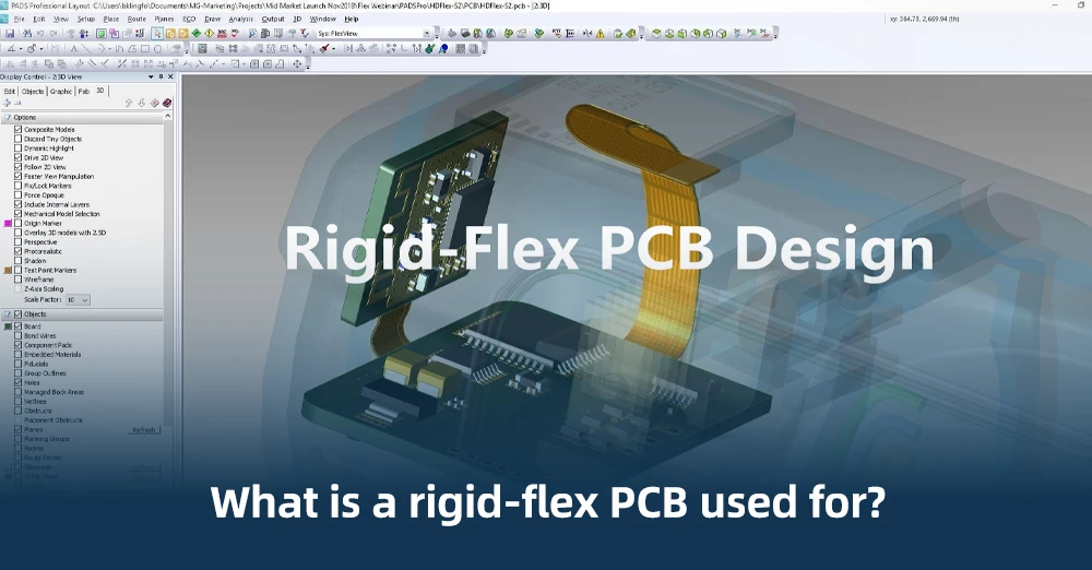
Rigid flex PCBs find applications in various industries and devices where their unique properties are beneficial. Here are some common uses:
Aerospace and Defense:
Avionics: Rigid flex PCBs are used in aircraft systems due to their ability to withstand vibrations, reduce weight, and fit into confined spaces.
Missile Systems: They’re employed in missile guidance systems for their reliability and ability to endure harsh conditions.
Medical Devices:
Implantable Devices: Rigid flex PCBs are used in medical implants due to their flexibility, enabling them to conform to the body’s contours while maintaining stability.
Diagnostic Equipment: Medical equipment like ultrasound machines, scanners, and monitoring devices utilize rigid-flex boards for compactness and durability.
Consumer Electronics:
Wearables: Devices like smartwatches, fitness trackers, and other wearables benefit from the flexibility and space-saving design of rigid-flex PCBs.
Mobile Devices: Smartphones and tablets use them to accommodate complex internal layouts and save space.
Automotive:
Automotive Electronics: Rigid flex PCBs are used in vehicles for their ability to withstand temperature variations, vibrations, and space-saving benefits in car electronics and control systems.
Industrial and Commercial Applications:
Robotics: In robotics and automation systems, where compactness, reliability, and durability are crucial, rigid-flex PCBs are employed.
Instrumentation: Test and measurement equipment, as well as industrial control systems, use them for their robustness and space-saving design.
Military and Defense:
Military Electronics: In defense systems, such as communication devices, radar systems, and ruggedized equipment, where reliability and durability are paramount.
General Electronics:
High-End Electronics: High-performance computing systems, servers, and high-speed data transmission applications benefit from their improved signal integrity and compactness.
Rigid flex PCBs are chosen for applications where standard rigid or flexible boards might not suffice due to space constraints, complex designs, or demanding environmental conditions. Their ability to offer a balance between flexibility, durability, and space optimization makes them suitable for a wide range of specialized applications across various industries.
What is the difference between rigid flex PCB and half flex PCB?
Rigid flex PCB and half-flex PCB are both configurations used in circuit board design, but they differ in their construction and flexibility:
* Rigid-Flex PCB:
Construction: Rigid flex PCBs combine rigid and flexible portions within a single board. They consist of both rigid sections (typically made of FR4 or similar rigid materials) and flexible sections (polyimide or similar flexible substrates) that are interconnected.
Flexibility: Rigid flex PCBs offer continuous flexibility throughout the flexible portions, allowing them to bend or fold as needed without compromising the circuitry or connections.
Design Complexity: These boards are complex to design and manufacture due to the integration of both rigid and flexible materials, and they provide a three-dimensional design capability.
* Half-Flex PCB:
Construction: Half-flex PCBs, on the other hand, feature a combination of rigid and flexible materials but in a different manner. They typically have a rigid portion and a flexible tail or connector.
Flexibility: The flexible part in a half-flex PCB is limited to a specific section, often used for connecting to other components or boards, but it doesn’t provide continuous flexibility throughout the board.
Design Complexity: While they may be easier to design compared to full rigid-flex boards, they still require specific considerations for the transition between the rigid and flexible sections.
Differences:
Flexibility Continuity: Rigid flex PCBs offer continuous flexibility throughout the designated flexible areas, while half-flex PCBs usually have flexibility limited to a specific section, such as a tail or connector.
Design Complexity: Rigid-flex PCBs are more complex in design and manufacturing due to their integrated rigid and flexible sections, while half-flex PCBs are somewhat simpler but still require attention to the transition between rigid and flexible areas.
Applications: Rigid-flex PCBs are often used in applications where complex three-dimensional designs and continuous flexibility are required. Half-flex PCBs are suitable for applications where flexibility in specific areas for connection purposes is necessary, but not throughout the entire board.
How are rigid flex PCBs made?
The manufacturing process for rigid flex PCB involves several intricate steps that integrate both rigid and flexible substrates into a single board. Here’s an overview of the process:
1. Design:
Design and Layout: Engineers create the PCB layout considering the rigid and flexible portions, ensuring they fit and function seamlessly.
2. Material Preparation:
Selection of Materials: High-quality rigid and flexible materials (like FR-4 for rigid sections and polyimide for flexible parts) are chosen based on the design specifications.
Copper Foil Preparation: Copper foil is applied to the rigid and flexible substrates, which will later form the conductive traces.
3. Imaging and Etching:
Photoresist Application: A photoresist layer is applied to the copper-clad substrates.
Imaging: The PCB design is transferred onto the photoresist using a photographic process.
Etching: Acid or chemical etching removes excess copper, leaving behind the desired circuit traces.
4. Drilling:
Precision Drilling: Holes are drilled in specific locations for component placement and interconnections between layers.
5. Plating:
Through-Hole Plating: Copper is plated inside the drilled holes, ensuring electrical connections between layers.
Surface Finishing: Surface finishes like ENIG (Electroless Nickel Immersion Gold) or HASL (Hot Air Solder Leveling) are applied to protect copper traces and facilitate soldering.
6. Lamination:
Rigid-Flex Lamination: The rigid and flexible layers are combined and bonded together under heat and pressure, forming a single, cohesive board.
Adhesive Application: Adhesive layers may be used to ensure the bond between rigid and flexible portions.
7. Solder Mask and Silkscreen:
Solder Mask: A protective layer is applied over the copper traces, leaving exposed areas for soldering components.
Silkscreen Printing: Component labels, identifiers, or logos are printed on the board’s surface for assembly guidance.
8. Component Mounting:
SMT (Surface Mount Technology): Automated machines precisely place and solder surface-mounted components on the rigid sections.
Through-Hole Component Assembly: Through-hole components are manually or robotically placed and soldered on both rigid and flex portions.
9. Testing and Inspection:
Electrical Testing: Boards undergo rigorous testing to ensure functionality and proper connectivity of all components and traces.
Visual Inspection: Manual inspection checks for any defects or anomalies in the board.
10. Final Processing:
Routing and Profiling: The boards are cut to their final shape, and any excess material is removed.
Cleaning: Boards undergo a cleaning process to remove residues and ensure optimal performance.
What materials are used in rigid flex PCB?
Rigid flex PCBs are constructed using a combination of materials that cater to the rigid and flexible sections of the board. Here are the primary materials commonly used in manufacturing rigid flex PCB:
Rigid Materials:
FR-4 (Fiberglass-Reinforced Epoxy Laminate): This material is the standard choice for rigid sections due to its excellent electrical insulation properties and durability.
Rigid Copper Foil: Copper foil is used to create conductive traces on the rigid sections, providing robust electrical connectivity.
Flexible Materials:
Polyimide (PI): Polyimide is a popular choice for flexible portions due to its flexibility, high-temperature resistance, and excellent dielectric properties.
Adhesive Materials: Adhesives are applied between layers to bond rigid and flexible sections, ensuring mechanical stability and preventing delamination.
Additional Materials:
Copper Foil for Flex Areas: Similar to rigid sections, copper foil is applied to flexible substrates to create conductive traces.
Solder Mask: Protective layers are applied over the conductive traces, leaving exposed areas for soldering components.
Surface Finish Materials: Surface finishes like ENIG (Electroless Nickel Immersion Gold) or HASL (Hot Air Solder Leveling) are applied for surface protection and solderability.
Adhesiveless Materials: Some rigid flex PCBs use special laminates that eliminate the need for adhesive layers, reducing overall thickness and enhancing flexibility.

How to design rigid flex PCB ?
Designing a rigid flex PCB requires a methodical approach and understanding of both rigid and flexible PCB design principles. Here are the key steps involved in designing a rigid-flex PCB:
Planning and Preparation:
Requirements Gathering: Understand the application’s requirements, including space constraints, environmental conditions, and necessary flexibility.
Component Placement Strategy: Plan the placement of components considering the rigid and flexible areas. Allocate components based on their sensitivity to mechanical stress.
Layer Definition: Define the layers needed for both rigid and flexible sections, considering the number of layers, material types, and thicknesses required.
CAD Software and Design Guidelines:
Use Specialized CAD Tools: Utilize PCB design software that supports rigid-flex design. These tools often have specific features for defining rigid and flexible areas, layer stackup, and routing considerations.
– Layer Stackup Definition:
a. Rigid Areas: Define the layer stack for the rigid portions of the board, considering standard PCB stackup guidelines.
b. Flex Areas: Specify the stackup for flexible portions, selecting appropriate flexible materials and thicknesses.
– Routing and Trace Considerations:
Define Bend Areas and Constraints:
a. Flex Bends: Mark areas where the board will bend or flex. Ensure no critical traces or components are placed in these areas to prevent damage during flexing.
– Route Traces Carefully:
a. Trace Routing: Route traces in rigid sections following standard PCB routing guidelines.
b. Flex Trace Routing: For flexible areas, use gradual curves and avoid sharp angles to minimize stress on traces during bending.
– Via Placement:
a. Via Types: Utilize appropriate vias (such as blind or buried vias) for transitions between rigid and flexible sections, ensuring signal integrity and reliability.
Design Verification:
– Design Rule Checks (DRC):
a. DRC Analysis: Perform design rule checks specific to rigid-flex PCBs to ensure compliance with manufacturing and design guidelines.
– Simulations and Testing:
a. Signal Integrity Analysis: Conduct simulations to verify signal integrity, especially in areas transitioning between rigid and flexible sections.
b. Mechanical Testing: Simulate or physically test the board’s flexibility to ensure it meets the required bending or flexing criteria without compromising functionality.
Collaboration and Documentation:
– Collaboration with Fabricators:
a. Consultation: Collaborate with PCB manufacturers experienced in rigid flex PCB fabrication to ensure the design aligns with their capabilities and requirements.
– Documentation:
a. Detailed Documentation: Provide comprehensive documentation including layer stackups, bend radii, material specifications, and any special instructions for fabrication and assembly.
What is the minimum bend radius for a rigid flex PCB?
The minimum bend radius for a rigid flex PCB depends on various factors including the material used for the flexible portion, the number of layers, and the design specifications. However, there are general guidelines to consider:
Material Type:
For polyimide-based flexible materials: The minimum bend radius can be around 10 to 20 times the thickness of the flex material. For example, if the flex material is 0.1mm thick, the minimum bend radius could be between 1mm to 2mm.
Number of Layers:
More layers may decrease the flexibility, so the minimum bend radius might need to be larger for boards with higher layer counts.
Manufacturer Specifications:
PCB manufacturers often provide specific guidelines for minimum bend radii based on the materials they use and their manufacturing capabilities. It’s crucial to consult with the manufacturer during the design phase.
Design Considerations:
The design layout and placement of components should consider the bend radius to avoid stress on traces, vias, and components during flexing.
Key Points:
Smaller bend radii allow for tighter bends but might risk damaging the board or affecting its reliability over time.
Larger bend radii offer more flexibility and reduce the risk of damage to the board during flexing.
Conclusion
Rigid flex PCBs epitomize innovation, revolutionizing the electronics industry with their adaptability, reliability, and space-saving attributes. Their transformative impact across diverse sectors signifies a new chapter in electronics design, where flexibility meets stability, and creativity knows no bounds. As these boards continue to evolve, they promise to underpin a future where technology seamlessly integrates into our lives in ways previously unimaginable.

