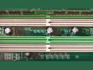
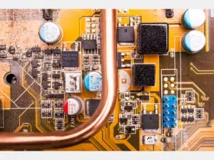
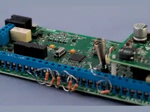
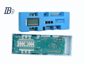
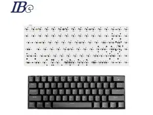
Which process should be done first, reflow soldering or wave soldering? This question mainly depends on the components on the circuit board. If the circuit board is full of chip components, then only the reflow soldering process is needed, and no wave soldering process is needed; if the circuit board is full of plug-in components, then the circuit board only needs the wave soldering process, and no reflow soldering process is needed; if the circuit board has both There are chip components and plug-in components, so the reflow soldering process must be done first and then the wave soldering process.
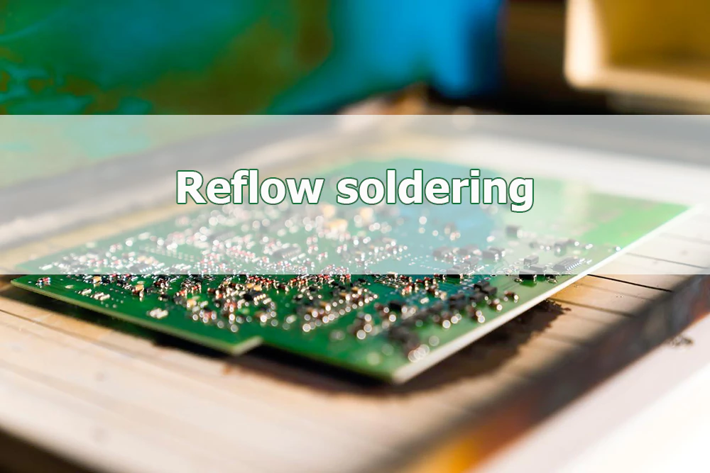
Reflow soldering
Reflow soldering is primarily used for Surface Mount Technology (SMT) components, including smaller-sized parts, ICs, and surface-mounted devices (SMDs).
Process:
Reflow soldering processes surface-mounted boards. The process is relatively complex and can be divided into two types: single-sided mounting and double-sided mounting.
A. Single-sided mounting: pre-coated solder paste → patch (divided into manual mounting and machine automatic mounting) → reflow soldering → inspection and electrical testing.
B.Double-sided mounting: Pre-coated solder paste on side A and one patch (divided into manual mounting and machine automatic mounting) → reflow soldering → Pre-coated solder paste on side B → SMT (divided into manual mounting and machine automatic mounting) Mounting)→reflow soldering→inspection and electrical testing.
Reflow soldering is a crucial process in PCB assembly for attaching Surface Mount Technology (SMT) components to a printed circuit board (PCB) using solder paste. Here are the basic steps involved:
1. Stencil Printing:
Solder Paste Application: A stencil is aligned over the PCB, and solder paste is applied through the stencil onto the PCB pads where the SMT components will be placed.
2. Component Placement:
Pick and Place: Automated machines or operators place SMT components onto the PCB according to the design layout.
3. Reflow Process:
• Ramp-Up: The temperature in the oven gradually rises, reaching the solder paste’s melting point. This phase eliminates moisture and preheats the assembly.
• Soak Zone: The assembly stays at a stable temperature, allowing the solder paste to fully melt and components to settle properly.
• Reflow Zone: This high-temperature zone ensures complete melting and soldering of the paste, creating secure solder joints between components and the PCB pads.
• Cooling Stage: The PCB exits the reflow oven and is cooled to solidify the solder joints.
4. Inspection:
Visual Inspection: The assembly is visually inspected for any defects, such as solder bridges, misaligned components, or insufficient solder.
5. Post-Soldering Processes:
Cleaning: If required, the PCB might undergo a cleaning process to remove any flux residues left from soldering.
Testing: Functional or electrical tests may be conducted to ensure the integrity and functionality of the assembled PCB.
6. Rework (if necessary):
Touch-up or Repair: Any defective solder joints or components are reworked or replaced.
Advantages:
Suitable for high-density components.
Allows precise control over the soldering process.
Suitable for double-sided PCBs with SMT components on both sides.
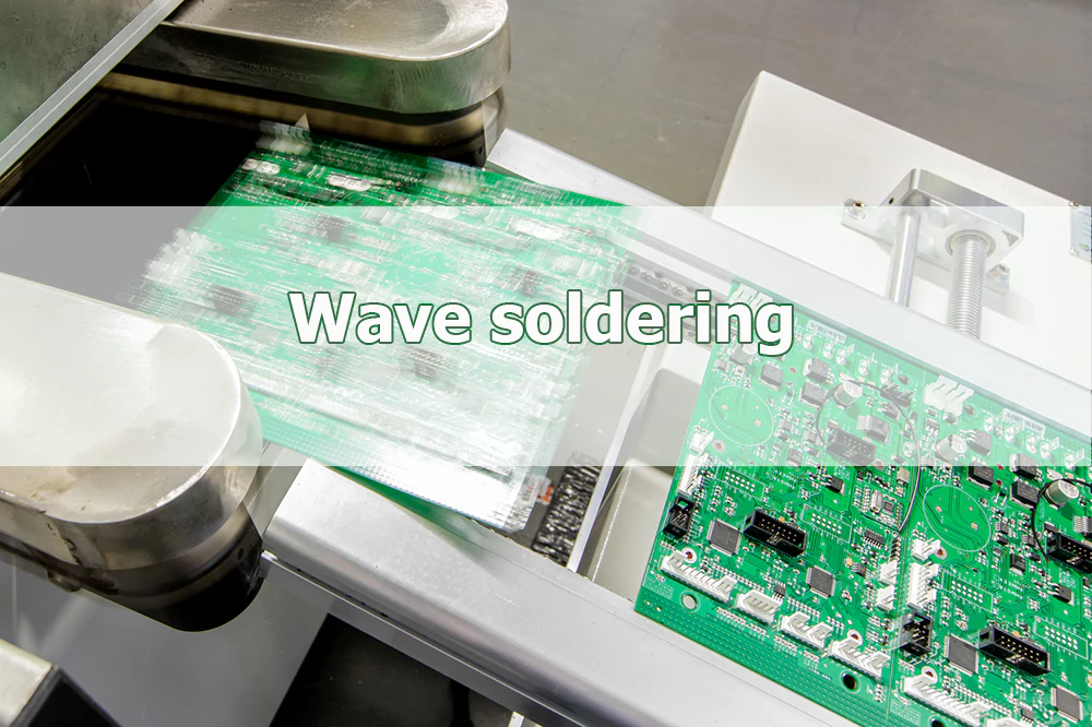
Wave soldering
Wave soldering is commonly used for Through-Hole Technology (THT) components that have leads passing through holes on the PCB.
Process:
Insert the component into the corresponding component hole → pre-coat flux → pre-bake (temperature 90-1000C, length 1-1.2m) → wave soldering (220-2400C) → cut off excess plug-in feet → check.
Wave soldering is a process used to solder through-hole components onto a printed circuit board (PCB). Here are the basic steps involved:
1. Flux Application:
Fluxing Stage: The PCB enters the fluxing chamber where a flux is applied to the areas where soldering will occur. Flux removes oxidation and helps facilitate solder wetting.
2. Preheating:
Preheat Zone: The PCB moves into a preheating section to gradually raise the temperature. This step removes moisture and preheats the PCB to prevent thermal shock during soldering.
3. Solder Application:
Wave Soldering: The PCB moves over a wave of molten solder, typically a tin-lead alloy. The through-hole components’ leads are immersed in this wave, soldering them to the board.
4. Cooling:
Cooling Stage: After passing through the solder wave, the PCB moves to a cooling area to solidify the solder joints.
5. Inspection:
Visual Inspection: The soldered PCB is inspected for defects like solder bridges, insufficient solder, or lifted component leads.
6. Post-Soldering Processes:
Cleaning (if needed): Some assemblies might undergo a cleaning process to remove flux residues left after soldering.
Testing: Functional or electrical tests may be performed to verify the functionality and integrity of the soldered PCB.
7. Rework (if necessary):
Touch-up or Repair: Any defective solder joints or components are reworked or replaced.
Advantages:
Efficient for soldering large volumes of through-hole components.
Generally faster and more cost-effective for THT components compared to manual soldering.

The reflow soldering chip components are all components with relatively small pins mounted on the circuit board, while the wave soldering components are relatively large plug-in components with pins, and the plug-in components are installed on the circuit board. The space is relatively large. If the wave soldering process is performed first, then the reflow soldering process of the chip components cannot be completed. Therefore, if the circuit board has both a reflow soldering process and a wave soldering process, the reflow soldering process must be performed first and then the wave soldering process.

