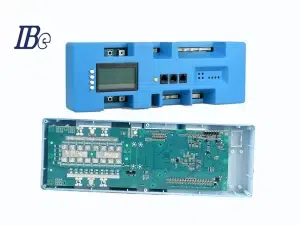
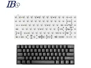
Solder mask ink is a very common and mainly used ink in PCB circuit boards. Generally, 90% of them are green, but there are also various colored inks.
The main function of solder mask ink is to protect and insulate the wires and components on the circuit board to prevent them from being damaged by environmental factors (such as moisture, corrosion, etc.).
At the same time, solder mask ink can also play a certain mechanical strengthening role, making the circuit board harder and more durable.
In addition, the surface of solder mask ink usually appears dark green or emerald green, which can be used as a mark to distinguish components and interfaces with different functions.
There are many reasons why the solder mask ink on printed circuit boards peels off. This article will explain the following reasons for you.
Why should circuit boards be coated with solder mask ink?
In the printed circuit board (PCB) manufacturing process, the coating of solder mask ink is a very critical process. The main function of the solder mask on the PCB board is to protect the circuit and prevent conductors from being stained with tin; to prevent electrical short circuits between conductors caused by moisture or chemicals; to prevent short circuits caused by improper handling of PCB boards in subsequent production processes and assembly; and the invasion of the PCB board by various harsh environments.
There are copper layers on both sides of the PCB board. The PCB board without solder mask is easily oxidized when exposed in the air and becomes a defective product, which also affects the electrical performance of the PCB board. Therefore, there must be a protective coating on the surface of the PCB circuit board that can block the oxidation reaction between the PCB and the air, and this coating is a solder mask covered with ink. Various colors of solder mask ink have also emerged, forming colorful PCB circuit boards, and the solder mask ink color has nothing to do with the quality and electrical performance of the PCB board.
Electronic components need to be soldered on the surface of the PCB board, so part of the copper layer needs to be exposed to facilitate soldering of components. This part of the copper layer is the soldering pad. Exposed copper layers are prone to oxidation reactions, so the pads also need a protective layer to prevent oxidation.
Why does the solder mask ink on the PCB peel off ?
One of the things that PCB ink often encounters in actual production is the falling off of solder mask ink on the circuit board. So what causes the soldering mask ink to fall off? How to avoid this phenomenon?
1. Aging or deterioration of the solder mask material: Over time, the material used in the solder mask will decompose or deteriorate, causing it to lose its ability to resist solvents and oils. This will cause the solder mask ink to peel off.
2. Contact with harsh chemicals: If the PCB (Printed Circuit Board) comes into contact with harsh chemicals or solvents, it may cause the solder mask to crack and lose its protective properties, causing the ink to fall off.
3. Solder mask is of poor quality or used improperly: If the solder mask material is of poor quality or used improperly, it may not adequately protect the PCB. This can lead to ink leaks and other problems.
4. Overheating: If the printed circuit board is exposed to high temperatures for a long time, it may cause the solder mask material to decompose, resulting in ink to fall off.
Generally speaking, the main reason for the ink peel off of the printed circuit board solder mask is the destruction of the protective properties of the solder mask material, which can be caused by a variety of factors, such as aging, exposure to harsh chemicals, poor quality, application Improper and overheating.
How to repair the ink loss on the pad?
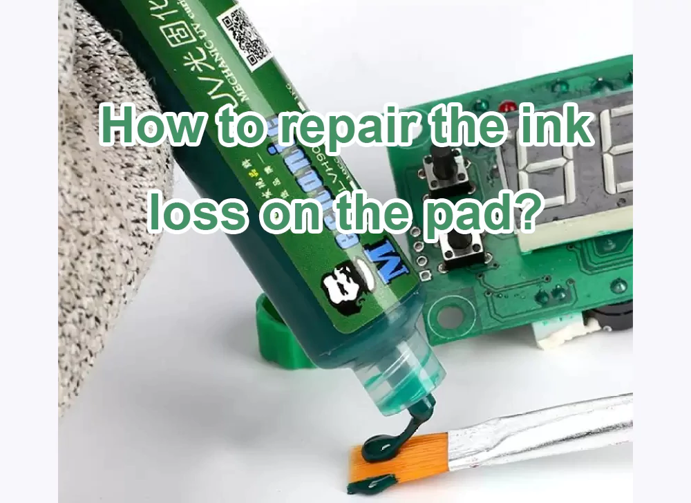
Generally speaking, it is difficult to repair the pad ink loss on the solder mask that has occurred, because this loss is usually caused by the breakage or damage of the pad protective layer material. However, you can take the following steps to reduce pad ink loss:
1. Use high-quality pad protection materials: Make sure to use high-quality, well-tested pad protection materials,which can reduce the risk of pad loss.
2. Avoid using overly aggressive cleaners: Use a mild cleaner to clean printed circuit boards and avoid using overly aggressive chemicals or cleaners. This can help protect the pad shield material from damage.
3. In addition, to control the temperature of the printed circuit board, the following measures can be used:
1. Use a heat sink or fan on the printed circuit board to reduce the temperature;
2. Avoid placing printed circuit boards in direct sunlight or in high temperature environments;
3. Control the power and working time of the heating element to avoid overheating the PCB board;
4. Use thermal insulation material around the heating element to reduce the temperature rise of the PCB board.
5. Finally, ensure the correct construction and application of pad protective layer materials.
If you follow these measures, you can reduce the risk of ink loss and ensure the quality and stability of your printed circuit board.

