Printed Circuit Boards (PCBs) are the backbone of most electronic devices, providing the essential connectivity for electronic components. As technology advances, the complexity of PCBs increases, making thorough testing and debugging crucial. One of the key elements in PCB design for effective testing is the inclusion of test points. Test points are designated areas on a PCB where measurements can be taken to ensure the proper functioning of the circuit. This essay explores the importance of PCB test point, its design considerations, and best practices for its implementation.
What is a test point in PCB?
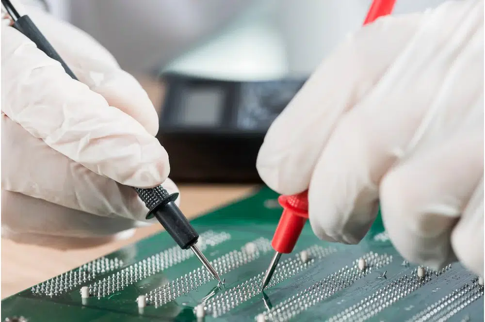
A test point on a printed circuit board (PCB) is a designated location where measurements can be taken or tests can be conducted. Test points are typically used to monitor the operation of a circuit, verify signal integrity, or diagnose issues. They are often labeled and designed to be easily accessible, allowing engineers or technicians to connect test equipment like oscilloscopes, multimeters, or logic analyzers.
Why are test points important?
PCB test points serve several critical functions in the design, manufacturing, and maintenance of electronic circuits.
1. Debugging and Troubleshooting: Test points are essential during the debugging phase of PCB design. They allow engineers to measure voltages, currents, and signals at various locations on the board, helping identify issues such as shorts, opens, or incorrect signal levels. Without test points, diagnosing and fixing problems can be time-consuming and challenging.
2. Quality Control and Assurance: During manufacturing, test points facilitate automated testing processes. Automated Test Equipment (ATE) can probe these points to verify that the board meets design specifications. This helps ensure that defective boards are identified and rejected before they reach the end-user, reducing the risk of failure in the field.
3. Maintenance and Repairs: For field repairs and maintenance, test points provide a convenient way for technicians to check the operational status of a board. This is particularly valuable for complex systems where manual inspection might be impractical.
4. Design Validation: In the prototype stage, test points enable designers to validate the circuit’s performance against design expectations. This helps in refining the design before mass production.
What’s the characteristic of PCB test point ?
Accessibility: Test points are placed in locations where they can be easily accessed without interfering with other components or circuit functions.
Designated Areas: They are often marked with specific symbols or labels on the PCB layout to clearly identify them.
Probe Points: They are designed to be compatible with test probes, allowing for straightforward connections.
Signal Monitoring: They may be used to monitor various types of signals such as power, ground, analog signals, or digital signals.
Troubleshooting: They are crucial for diagnosing issues during development, manufacturing, or repair of the PCB.
How to use PCB test point ?
Using PCB test points effectively involves several steps, primarily focused on measurement, verification, and troubleshooting. Here’s a guide on how to use them:
1. Identify Test Points
Locate Test Points: Look at the PCB schematic or layout to find designated test points. They are often marked with labels or symbols, and you may also find them in the documentation or design files.
Check Labels: Test points may be labeled with names or numbers indicating their purpose or the type of signal they carry (e.g., Vcc, GND, Signal A, etc.).
2. Select Appropriate Test Equipment
Multimeter: For measuring voltage, current, or resistance.
Oscilloscope: For analyzing waveforms, signal integrity, and timing issues.
Logic Analyzer: For digital signals, helping to monitor and analyze complex data patterns.
Probes: Use appropriate probes or test leads compatible with your test equipment.
3. Connect to Test Points
Ensure Proper Contact: Attach test probes or leads to the test points. Make sure there is a secure and reliable connection to avoid false readings or intermittent contact.
Minimize Interference: Be cautious about potential interference from other components or signals. Ensure that the connection does not short any circuits or affect the normal operation of the PCB.
4. Perform Measurements
Voltage Measurement: Measure the voltage at power rails, signal lines, or other critical nodes to ensure they are within expected ranges.
Signal Analysis: Use an oscilloscope to capture and analyze waveform characteristics, such as frequency, amplitude, and noise. This helps in understanding the behavior of signals over time.
Continuity and Resistance: Check for continuity in traces and components to ensure there are no open circuits or shorts.
5. Analyze Results
Compare with Specifications: Compare your measurements with the expected values or specifications in the design documentation.
Look for Anomalies: Identify any discrepancies, noise, or irregularities in the data that may indicate issues such as component failures, design flaws, or interference.
Where do you put test points?
Test points should be placed strategically on a PCB to facilitate effective testing and debugging. Here are key considerations for optimal placement:
1. Critical Signals: Place test points near critical signal paths and important nodes, such as data lines, clock signals, and high-speed interfaces, where measurements are crucial for diagnosing issues.
2. Power and Ground: Position test points at key points in the power distribution network and ground connections to monitor voltage levels and verify proper power distribution.
3. Component Pins: Place test points near important component pins, especially those involved in key functions or sensitive areas, to simplify checking component performance.
4. Test Access Points: Ensure test points are located where they are easily accessible without interfering with other components or mechanical parts. They should be placed so that they can be probed without requiring excessive disassembly.
5. High-Risk Areas: Include test points in areas of the circuit that are prone to faults or have a higher likelihood of failure. This allows for easier troubleshooting in problematic regions.
6. Boundary Conditions: For circuits with boundary conditions or interfaces, place test points at these boundaries to verify correct signal behavior and interactions.
7. Designated Areas: Use designated areas or test zones on the PCB layout specifically for test points, ensuring they do not overlap with critical signal routes or impede component placement.
8. Automated Testing: For automated testing, align test points with the probe grid of Automated Test Equipment (ATE) to ensure compatibility and ease of use.
By considering these factors, you ensure that test points are effectively integrated into the PCB design, facilitating easier and more accurate testing and debugging.
What is the spacing for test points in PCB?
The spacing for test points in a PCB depends on several factors including the type of test equipment used, the size of the test probes, and industry standards. Generally:
For Manual Testing: Test points should be spaced far enough apart to allow easy access with standard test probes. Typically, a minimum spacing of 0.1 to 0.2 inches (2.5 to 5 mm) between test points is recommended.
For Automated Testing: When designing for Automated Test Equipment (ATE), follow specific guidelines provided by the equipment manufacturer. This often involves spacing test points at regular intervals, such as 0.1 inches (2.54 mm) or multiples thereof, to align with the ATE probe grids.
Signal Integrity Considerations: For high-speed or high-frequency signals, ensure that the spacing minimizes signal interference and maintains signal integrity. Spacing should be adequate to avoid crosstalk and maintain performance.
Standard Guidelines: Adhere to industry standards, such as IPC-2221, which provide guidelines for spacing and pad sizes based on the test equipment and PCB design requirements.
Conclusion
PCB test points are a fundamental aspect of PCB design, providing crucial benefits for debugging, quality control, maintenance, and design validation. By carefully considering their design and implementation, engineers can enhance the reliability and functionality of electronic devices. Adhering to best practices and industry standards ensures that test points contribute effectively to the overall performance and manufacturability of PCBs. As technology continues to evolve, the role of test points will remain integral to the successful development and maintenance of electronic systems.
A test point on a printed circuit board (PCB) is a designated location where measurements can be taken or tests can be conducted. Test points are typically used to monitor the operation of a circuit, verify signal integrity, or diagnose issues.
Debugging and Troubleshooting
Quality Control and Assurance
Maintenance and Repairs
Design Validation
Critical Signals
Power and Ground
Component Pins
Test Access Points
High-Risk Areas
Boundary Conditions
Designated Areas
Automated Testing

