In the manufacturing process of electronic products, PCB as a carrier of electronic components and realize its electrical connection of the core carrier, its quality directly affects the performance and stability of the product. In order to ensure that the quality of PCB circuit boards in line with the design requirements, various types of specialized test fixtures and instruments came into being. This article will unveil the mystery of PCB test for you, and detailed introduction to those in the production line plays a key role in the jig instrument.
What is PCB test?
PCB test, also known as printed circuit board testing, is a crucial process in the manufacturing of electronic devices. It involves verifying the functionality and quality of the printed circuit board (PCB) before it is assembled into the final product. PCB testing helps ensure that the electronic device operates correctly, meets specifications, and is free from defects.
What do the PCB tests include?
Functional Testing
In-Circuit Testing (ICT)
Automated Optical Inspection (AOI)
In-Circuit Emulation (ICE)
Boundary Scan Testing
Burn-In Testing

Why need PCB test?
PCB testing is essential for ensuring the quality, reliability, and functionality of electronic devices by detecting and resolving defects early in the manufacturing process. It helps minimize the risk of faulty products reaching the market and ensures customer satisfaction with the final product.
PCB testing is essential for several reasons:
• Quality Assurance: PCB testing helps ensure that the manufactured PCBs meet the required quality standards.
• Reliability: Electronic devices rely on PCBs to function correctly. PCB testing helps identify potential issues that could affect the reliability and longevity of the device, such as faulty components, soldering defects, or electrical shorts.
• Compliance: Many industries have strict regulations and standards regarding the quality and safety of electronic devices. PCB testing ensures that the manufactured PCBs comply with these standards, helping manufacturers avoid legal and regulatory issues.
• Cost Reduction: Identifying and addressing defects early in the production process through PCB testing helps reduce the overall cost of manufacturing.
• Risk Mitigation: PCB testing helps mitigate the risk of product failures and recalls, which can have significant financial and reputational consequences for manufacturers.
What instruments and machines are required for the PCB test?
Flying Probe Tester
The Flying Probe Tester is a non-contact, fixtureless PCB testing device. It automatically locates the test points using multiple sets of movable fine probes and conducts electrical signal detection according to preset test procedures. The Flying Probe Tester is particularly suitable for testing PCBs with small batches, high density, and complex structures. It does not require the production of special fixtures and offers the advantages of high flexibility and short testing cycles.
In-Circuit Tester (ICT)
The In-Circuit Tester is a PCB functional testing device based on dedicated test fixtures. First, it is necessary to produce corresponding ICT test fixtures according to the PCB design. These fixtures contain probes precisely aligned with each test point on the PCB. During testing, the PCB is fixed in the fixture, and the probes make contact with each test point. The ICT system loads electrical signals and monitors responses to detect solder joint connectivity, component parameters, and circuit functionality. ICT testing has high precision and effectively detects problems at the soldering and component levels. However, fixture costs are relatively high, making it suitable for large-scale production of stable products.
Automated Optical Inspection (AOI)
AOI equipment utilizes high-resolution cameras and advanced image processing technology to conduct comprehensive visual scans of PCBs. It detects defects such as missing components, misalignment, tombstoning, bridging, insufficient or excess solder, etc. AOI is fast, efficient, non-contact, and does not damage the PCB. It is commonly used for real-time quality monitoring on SMT production lines.
X-ray Inspection System
Conventional optical inspection methods struggle to penetrate packaging forms such as BGA and CSP or hidden solder joints within PCBs. In such cases, the X-ray Inspection System proves valuable. It penetrates the PCB with X-rays, generating perspective images of internal structures. This allows clear observation of solder joint shapes, voids, bridging, and other potential defects, providing strong assurance for high-quality PCB manufacturing.
Functional Test Fixture
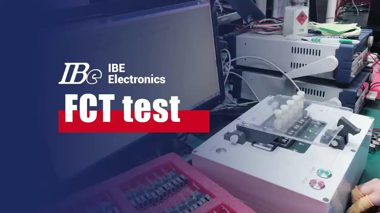
Functional Test Fixtures are primarily used to simulate actual working environments and conduct comprehensive functional verification of assembled PCBs. These fixtures typically include power supplies, signal sources, loads, simulators, etc., along with connectors matching the PCB interface. By executing specific test procedures, they check whether the PCB functions meet design requirements. Functional testing can identify logic errors, interface compatibility issues, and other deep-seated faults, serving as the final line of defense for product quality control.
Thermal Shock Chamber
Although not directly related to circuit testing, the Thermal Shock Chamber is crucial for evaluating the reliability and durability of PCBs under extreme temperature changes. It simulates rapid and substantial temperature changes, detecting performance changes, solder joint strength, material aging, etc., during thermal cycling. This ensures that products can operate stably in various harsh environments.
Conclusion
In summary, there is a wide variety of PCB testing fixtures and instruments, each with its own strengths. They cover multiple dimensions from basic electrical performance testing and appearance defect identification to in-depth functional verification and environmental tolerance assessment. Choosing and utilizing these fixtures and instruments appropriately is crucial to ensuring high-quality PCBs and stable performance of electronic products.
PCB test, also known as printed circuit board testing, is a crucial process in the manufacturing of electronic devices. It involves verifying the functionality and quality of the printed circuit board (PCB) before it is assembled into the final product.
Functional Testing
In-Circuit Testing (ICT)
Automated Optical Inspection (AOI)
In-Circuit Emulation (ICE)
Boundary Scan Testing
Burn-In Testing
PCB testing is essential for ensuring the quality, reliability, and functionality of electronic devices by detecting and resolving defects early in the manufacturing process. It helps minimize the risk of faulty products reaching the market and ensures customer satisfaction with the final product.


