IC package, to put it simply, is to place the integrated circuit bare chips produced by the manufacturer on a carrier substrate, then lead out the pins, and then fix and package them into a whole.
It can protect the chip and is equivalent to the shell of the chip. It can not only fix and seal the chip, but also enhance its electrothermal performance. Therefore, packaging plays a very important role in CPUs and other large-scale integrated circuits.
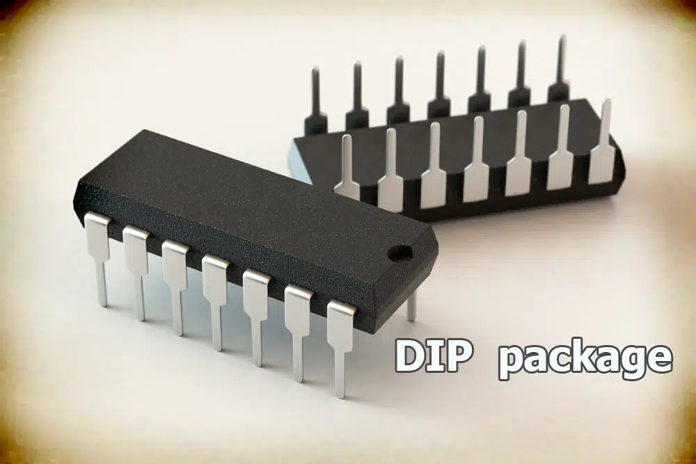
DIP package
DIP (direct plug-in package) refers to an integrated circuit chip packaged in dual in-line form. This chip package has a history of many years. For example, 51 microcontrollers, AC-DC controllers, optocoupler op amps, etc. all use this package type. The CPU chip packaged in DIP has two rows of pins and can be used through a special base. Of course, it can also be directly inserted into a circuit board with the same number of solder holes and geometric arrangement for soldering. For use on the base, it can be easy for replacement and welding, and only a soldering iron is needed for welding and assembly.
LQFP/TQFP package
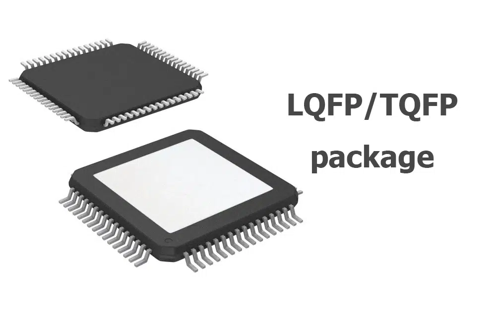
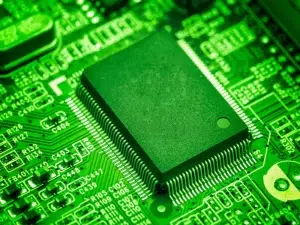
Many microcontrollers and integrated chips are currently using this kind of package. Since this package has protruding pins, care needs to be taken during transportation and welding to prevent the pins from being bent or damaged.
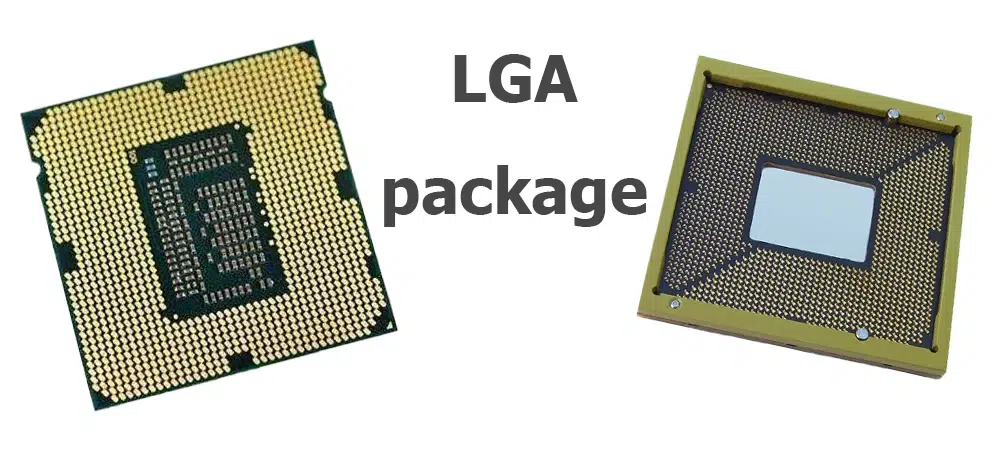
LGA package
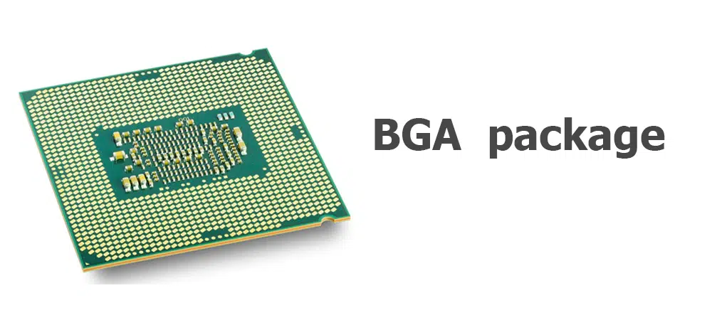
BGA package
With the advancement of integration technology, the improvement of equipment and the use of deep sub-micron technology, LSI, VLSI, and ULSI have appeared one after another. The integration level of silicon single chips has continued to increase, the requirements for integrated circuit packaging have become more stringent, and the number of I/O pins has increased sharply, and the power consumption also increases.
BGA (ball grid array) package is an electronic component packaging technology. It refers to packaging electronic components in a multi-layer spherical structure composed of metal and ceramics to provide better thermal conductivity and smaller package size. BGA packages can provide more connection points, several times more than ordinary plug-in packages, thus providing higher signal integrity and lower resistance. BGA package can also provide higher power density and lower electromagnetic interference (EMI).
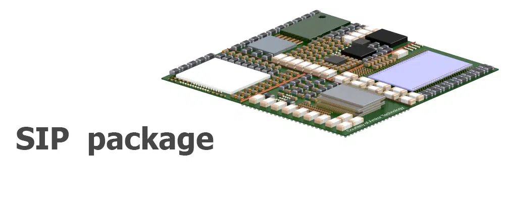
SIP package
SIP system-level packaging integrates multiple functional chips, including processors, memories and other functional chips, into one package to achieve a basically complete function. SIP packages correspond to SOCs, but their difference is that SIP packaging uses different chips to be packaged side by side or stacked, while SOC is a highly integrated chip product. From the perspective of packaging development, SIP is the basis for SOC packaging implementation.
SiP has a wide range of applications, mainly including: wireless communications, automotive electronics, medical electronics, computers, military electronics, etc.
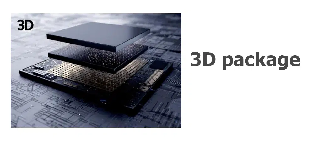
3D package
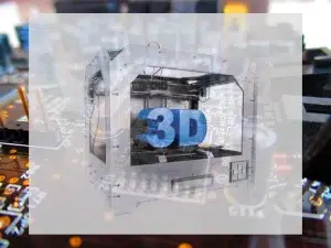
3D package is an advanced integrated circuit packaging technology that stacks multiple chips or devices vertically to achieve smaller, more compact package sizes. This technology can significantly improve the performance, functionality and reliability of electronic devices while also reducing costs.
Classification:
1: The packaging trend is package-on-package (PoP); low-yield chips seem to be leaning towards PoP.
2:Multi-chip packaging (MCP) method. high-density and high-performance chips tend to use MCP.
3:Mainly based on system-in-package (SiP) technology, in which logic devices and memory devices are manufactured in their own processes and then combined together in a SiP package.

