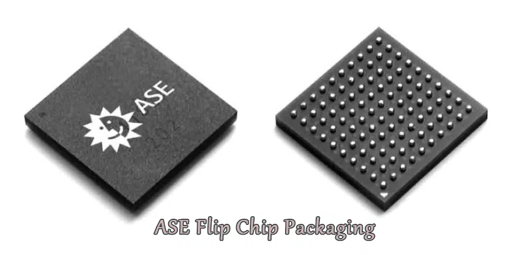
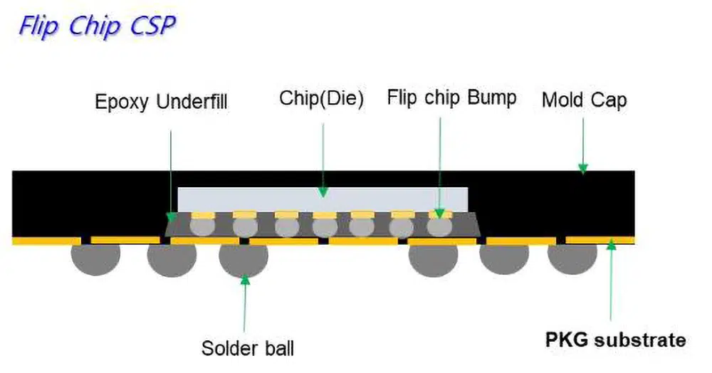
FC-CSP is one of the Chip Scale Package (CSP) types. According to the definition of the J-STD-012 standard, CSP refers to a packaging form in which the size of the package does not exceed 1.2 times that of the bare chip. It realizes the electrical interconnection between the chip and the substrate through flip-chip welding of the bump and the substrate, the chip faces downward, and the chip welding area and the substrate welding area are directly interconnected.
Compared with WB and TAB bonding methods, the distance between the semiconductor chip and the substrate in FC-CSP is smaller, the signal loss is reduced, and the I/O density is high, which is more suitable for Large-scale Integration (LSI), Very Large Scale Integration(VLSI) and Application Specific Integrated Circuit (ASIC) chips.
Features of FC-CSP
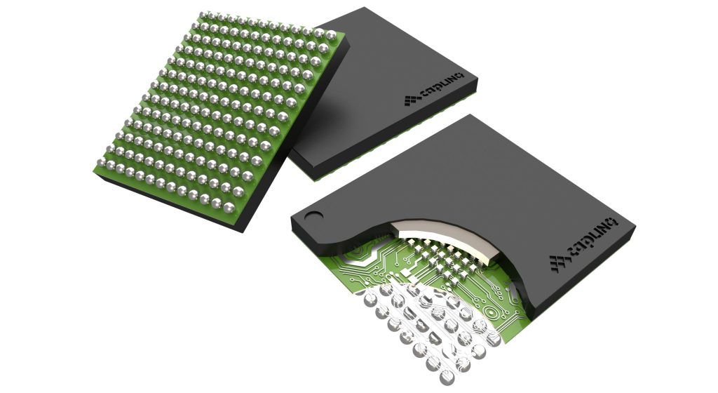
As an advanced packaging technology, FC-CSP mainly has the following technical features:
(1) Smaller package size: the package area of FC-CSP is less than 1/10 of that of QPP (0.5mm pitch), and only 1/3~1/10 of that of BCA package; especially when using copper bump package, it can further reduce the bump pitch, thereby reducing the package area.
(2) More pins (I0): In a chip package of the same size, FC-CSP can accommodate more pins than traditional wire-bonded packages.
(3) Better electrical performance: due to the shorter interconnection between the chip and the package casing wiring, smaller parasitic parameters, smaller signal interference, and shorter signal transmission delay time, it has smaller resistivity and faster signal transmission speed.
(4)Realize the integrated packaging of various chips and devices with different functions.
Key technologies of FC-CSP
(1)FC-CSP has high requirements for the thickness of the package, so when the wafer is thinned, it is necessary to strictly control the final thickness (within the target value ±151μm). In addition, the process parameters must be well controlled to avoid problems such as product chip fragments and cracks during cutting .
(2)Since reflow soldering is used to connect the chip bumps and the circuit of the substrate, it is necessary to prevent open circuit during reflow and short circuit when the pitch is too small. Especially when the area of the chip and the substrate is relatively large, due to the difference in the heat shrinkage ratio of the chip and the substrate material, it may cause warpage during high-temperature reflow soldering, thereby generating a certain stress, resulting in breakage at the connection between the bump and the substrate.
(3) The cooling rate of reflow soldering must be strictly controlled to avoid the fracture of the joint between the bump and the substrate and the low-K material in the wafer. Generally, when the temperature drops below 150 degrees Celsius, the cooling rate should be controlled within 4 degrees Celsius/s.
(4) When the bump and the circuit on the substrate are narrow, the amount of tin on the bump and the accuracy of flip-chip alignment must be strictly controlled to prevent the short circuit caused by the connection between the bump and the adjacent substrate circuit.
(5) After flip-chip mounting, a plastic package must be used and cured to protect the internal chip, and also play a role in blocking external signal interference. The curing time and temperature during the plastic packaging process must be strictly controlled to avoid the separation of the plastic package and the chip, and the occurrence of product warpage after plastic packaging.
Combining the technology and the current research and development of various IC manufacturers, the main structure types of FC-CSP are Single Die FC-CSP, Muli-Chip Side byside FC-CSP and Stacked-Die Hybrid FC-CSP. Stacked packaging refers to stacking multiple chips on a core cavity or substrate, and connecting chips to chips or packages. Stacked packaging is mainly used in mobile phone processors to reduce power consumption, reduce size, and improve packaging integration and performance.
Applications of FC-CSP technology
With the rapid promotion of FC-CSP technology, its application is becoming more and more extensive. The main application fields are as follows :
(1) Consumer electronics: mobile phones, camcorders, digital electronics, DVDs, wireless products, etc.
(2) Computers: voltage regulators, high-speed memory, smart cards, peripherals, etc.
(3) Communication category: digital pager, mobile phone, CPS, etc.
(4) Because of its high pin count, miniaturization, miniaturization, thinness, multi-function and other characteristics, FC-CSP is widely used in network communication, digital signal processing, mixed signal and radio frequency signal, application-specific integrated circuit, micro-control devices and so on.


