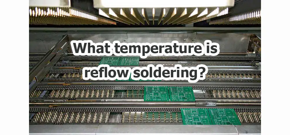
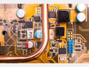
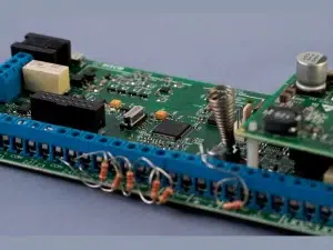
Reflow soldering is a widely used technique in electronics manufacturing for joining surface mount components to printed circuit boards (PCBs). It involves the precise application of solder paste followed by a controlled heating process to create reliable electrical connections between components and the PCB.
What are the types of soldering?
In PCB manufacturing, various types of soldering methods are employed to join electronic components to the board. Here are some common types:
Reflow Soldering:
Description: Utilizes solder paste to temporarily attach surface mount components to the PCB.
Process: Components are positioned on solder paste-applied pads. The entire assembly is heated in a reflow oven, melting the solder paste and forming the connections.
Wave Soldering:
Description: Mainly used for through-hole components.
Process: PCB with through-hole components is passed over a wave of molten solder, which adheres to exposed metal areas, creating connections.
Hand Soldering:
Description: Manual process using a soldering iron for precise component placement and soldering.
Process: Components are individually placed and soldered onto the PCB using a soldering iron and solder wire.
Selective Soldering:
Description: Targets specific areas for soldering, suitable for mixed technology boards with both surface mount and through-hole components.
Process: Precisely directs solder to specific components or areas using a robotic soldering system.
Infrared Soldering:
Description: Uses infrared radiation to heat and melt solder, suitable for delicate or heat-sensitive components.
Process: Infrared emitters heat the solder joints without significantly affecting surrounding areas.
Vapor Phase Soldering:
Description: Utilizes the condensation of a vaporized solder to create a uniform soldering process.
Process: PCB is lowered into a vapor zone, and as it reaches a specific temperature, solder condenses on the PCB’s surfaces, forming connections.
Each soldering method has its advantages and is chosen based on factors such as component types, board design, production volume, and required precision. The selection of the soldering technique influences the quality, efficiency, and reliability of the final PCB assembly.

What is reflow soldering used for?
The primary function of reflow soldering is to create reliable and durable electrical connections between surface mount components and the printed circuit board (PCB) in electronic devices.
Reflow soldering is a widely used technique in PCB manufacturing for attaching surface mount components to the board. It’s primarily employed for:
1. Surface Mount Technology (SMT): Reflow soldering is the go-to method for SMT components, which lack leads or require precise positioning. This includes components like resistors, capacitors, ICs (integrated circuits), and smaller devices.
2. High-Volume Production: It’s well-suited for high-volume production due to its automation potential and efficiency in soldering multiple components simultaneously.
3. Miniaturized Electronics: With the trend toward smaller, compact electronics, reflow soldering allows for precise and reliable connections in confined spaces on the PCB.
4. Consistent and Reliable Connections: The controlled reflow process ensures consistent solder joints, minimizing defects and producing reliable electrical connections.
5. Rapid Production Cycles: Reflow soldering enables quick assembly processes, contributing to shorter manufacturing lead times for electronic devices.
6. Complex PCB Designs: It accommodates intricate PCB designs with numerous components, intricate layouts, and fine-pitched components.
Reflow soldering, with its precision, reliability, and suitability for modern electronics, has become a cornerstone technique in PCB assembly, especially for surface mount components.
What are the steps in reflow soldering?
The reflow soldering process consists of several key steps that ensure proper heating, melting, and solidification of solder paste to create reliable connections between components and the PCB. Here are the general steps involved in reflow soldering:
1. Solder Paste Application:
Dispensing: A solder paste, a mixture of solder alloy particles and flux, is applied precisely onto the PCB pads using a stencil or a dispensing system.
2. Component Placement:
Pick and Place: Surface mount components (SMDs) are accurately positioned on the solder paste-applied pads using automated pick-and-place machines.
3. Preheating (Preheat Zone):
Warm-up Phase: The PCB with components is preheated gradually to remove moisture and pre-activate the flux in the solder paste.
Reduces Thermal Shock: Preheating minimizes thermal shock during rapid temperature changes in subsequent stages.
4. Reflow Phase (Soldering Zone):
Ramp-up: Temperature rises rapidly to reach the reflow temperature, activating the flux and initiating solder melting.
Soak: The temperature is held at the reflow temperature to ensure complete solder melting and alloying between surfaces.
Cool Down: The PCB moves through the reflow oven, allowing the solder joints to solidify as the assembly cools down.
5. Cooling Phase (Cooling Zone):
Gradual Cooling: The PCB assembly gradually cools down as it moves through the cooling zone of the reflow oven.
Solidification of Solder: Solder joints solidify, forming strong connections between components and the PCB.
6. Inspection and Quality Control:
Post-reflow Inspection: Visual inspection or automated systems check for defects, ensuring proper soldering and component alignment.
The precise temperatures and duration at each stage are crucial, as variations can impact the quality of solder joints. These steps are meticulously controlled in a reflow oven to achieve consistent and reliable soldering results across multiple PCBs during high-volume production.
What is the difference between wave soldering and reflow soldering?
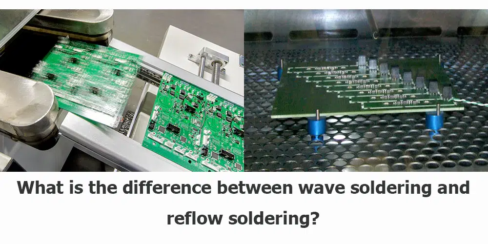
Wave soldering and reflow soldering are two distinct methods used in PCB assembly, each with its specific applications and processes:
| Wave Soldering | Reflow Soldering | |
|---|---|---|
| Process | Application: Primarily used for through-hole components on PCBs. Soldering Method: Involves a molten wave of solder that the PCB passes over, creating solder connections on exposed metal areas. | Application: Primarily used for surface mount technology (SMT) components. Soldering Method: Involves solder paste applied to the PCB pads, followed by heating the assembly in a reflow oven to melt and form solder joints. |
| Component Suitability | Through-Hole Components: Best suited for components with leads that pass through holes on the PCB. | Surface Mount Components: Ideal for components without leads, such as small ICs, resistors, capacitors, and other SMT parts. |
| Assembly Technique | Selective Process: Targeted at specific areas where soldering is required, particularly through-hole components, while other areas are protected. | Full Coverage: Entire PCB is subjected to the reflow process, ensuring solder connections on all SMT components simultaneously. |
| Heat Exposure | Localized Heating: Only components requiring solder are exposed to high temperatures during the wave soldering process. | Uniform Heating: The entire PCB and components experience uniform heating during the reflow process. |
Both methods have their advantages and are chosen based on the types of components, board design, and production requirements in the PCB assembly process. Often, a combination of both techniques is used to cater to mixed-technology PCBs with both through-hole and surface mount components.
What is the reflow profile of a PCB?
The reflow profile of a PCB refers to the temperature-time characteristics that define the heating and cooling stages during the reflow soldering process. It’s a critical parameter in ensuring proper soldering without damaging components or the PCB itself. The reflow profile typically consists of several key phases:
1. Preheat Zone:
Purpose: Eliminate moisture and activate the flux in the solder paste.
Temperature: Begins at ambient temperature, gradually ramps up to a preheat temperature (around 100-150°C).
Duration: Typically lasts for 60-180 seconds.
2. Thermal Soak or Soak Zone:
Purpose: Ensure uniform temperature across the entire PCB assembly.
Temperature: Ramps up further to the reflow temperature (usually between 200-250°C).
Duration: Held at the reflow temperature for a specific time (usually 30-120 seconds).
3. Reflow or Reflow Zone:
Purpose: Achieve complete melting and alloying of solder paste for proper solder joint formation.
Temperature: Reaches peak temperature (typically around 240-260°C) to fully liquefy the solder paste.
Duration: Kept at peak temperature for a brief period (10-60 seconds).
4. Cooling Zone:
Purpose: Gradual cooling to solidify solder joints and prevent thermal shock to components.
Temperature: PCB assembly gradually cools down to solidify solder joints (below 150°C).
Duration: Cooling period usually varies, depending on the specific cooling rate required for the components and the PCB.
Importance of Reflow Profile:
• Solder Joint Quality: Proper reflow profile ensures optimal wetting and bonding between solder paste, components, and PCB pads, resulting in strong, reliable solder joints.
• Component Integrity: Prevents overheating of sensitive components, reducing the risk of thermal damage or solder joint failure.
• Avoids Defects: Ensures consistent, defect-free soldering across the PCB assembly.
The reflow profile parameters (temperature, ramp rates, and durations) are carefully defined based on the solder paste specifications, component types, and the PCB’s thermal characteristics to achieve reliable soldering while preserving the integrity of components and the PCB itself.
What temperature is reflow soldering?
Reflow soldering involves a controlled heating process where the temperature varies at different stages to melt and solidify the solder paste. The specific temperatures used in reflow soldering depend on the solder paste type, component specifications, and the reflow profile. However, here are approximate temperature ranges commonly associated with reflow soldering:
Preheat Zone:
Temperature: 100-150°C (212-302°F)
Purpose: Eliminate moisture and activate flux in the solder paste.
Soak Zone:
Temperature: 200-250°C (392-482°F)
Purpose: Achieve uniform temperature across the PCB assembly.
Reflow Zone:
Peak Temperature: 240-260°C (464-500°F)
Purpose: Fully liquefy the solder paste for proper solder joint formation.
These temperature ranges can vary based on the specific solder paste and component requirements. It’s essential to follow the recommended reflow profile provided by the solder paste manufacturer to ensure optimal soldering results without damaging components or the PCB.
How do you clean PCB after reflow?
Cleaning a PCB after reflow soldering is crucial to remove residual flux, solder paste residues, and other contaminants that may affect the board’s reliability and functionality. Here’s a general guide for cleaning a PCB after reflow soldering:
1. Selection of Cleaning Method:
Cleaning Agents:
Water-Based Cleaners: Mild, environmentally friendly cleaners suitable for water-soluble fluxes.
Solvent-Based Cleaners: Stronger cleaners effective for no-clean or rosin-based flux residues.
Cleaning Equipment:
Batch Cleaning Machines: Used for larger-scale cleaning operations.
Ultrasonic Cleaners: Effective for smaller-scale cleaning or intricate areas.
2. Cleaning Process:
Preparation:
Ensure Safety: Use appropriate personal protective equipment (PPE) when handling cleaning agents.
Select Cleaning Agent: Choose the suitable cleaning agent based on the flux type and residues present.
Cleaning Steps:
a. Spray or Apply Cleaner:
Use a spray or apply the cleaning agent onto the PCB, ensuring coverage over all soldered areas.
b. Agitation (if applicable):
For batch cleaners or ultrasonic machines, activate the agitation process to help dislodge residues.
c. Rinse (if applicable):
If using a water-based cleaner, rinse the PCB with clean water to remove the cleaning agent.
d. Drying:
Ensure complete drying of the PCB before further handling or assembly. Air drying or using a drying oven can be employed.
3.Post-Cleaning Inspection:
Visual Inspection:
Inspect the PCB visually for any remaining residues, ensuring cleanliness.
Quality Control:
Perform electrical testing or quality checks to verify that the cleaning process hasn’t affected the PCB’s functionality.
Precautions:
• Follow the manufacturer’s recommendations for cleaning agents and methods.
• Ensure proper ventilation when using solvent-based cleaners.
• Avoid excessive scrubbing or aggressive cleaning methods that may damage components or the PCB.
• Adhering to appropriate cleaning procedures after reflow soldering helps maintain the integrity of the PCB, ensuring long-term reliability and functionality.
Conclusion
Reflow soldering is a fundamental process in modern electronics manufacturing, facilitating efficient and reliable assembly of electronic components onto PCBs with high precision and repeatability.
Reflow Soldering
Wave Soldering
Hand Soldering
Selective Soldering
Infrared Soldering
Vapor Phase Soldering
The reflow soldering process consists of several key steps that ensure proper heating, melting, and solidification of solder paste to create reliable connections between components and the PCB.
Key Differences:
Component Types: Wave soldering is primarily for through-hole components, while reflow soldering is for surface mount components.
Soldering Method: Wave soldering uses a wave of molten solder, while reflow soldering utilizes solder paste and a reflow oven.
Application Area: Wave soldering targets specific areas, while reflow soldering covers the entire PCB surface.
...

