As the core of modern electronic equipment, the production technology of circuit boards is more and more advanced. Blind and buried vias PCB is a widely used in electronic equipment and it combines the structure of multilayer PCB board and blind or buried hole technology, can achieve more complex circuit connection. This article will introduce in detail the definition and function of Blind and buried vias PCBs and explore their differences from traditional PCB boards.
What is the blind and buried vias PCB
Blind & buried vias PCB is a mainstream circuit board manufacturing technology, which adopts the structure of multi-layer PCB, punching blind holes on one side of the board or buried holes in multi-layer boards to achieve the connectivity of different layers of circuits. Generally, blind via board means that only one side of the board can pass through on both sides of the board, while for buried via board, both sides of the board are stacked and buried.
Compared to traditional PCB boards, blind and buried vias PCBs use stricter manufacturing standards and more sophisticated processes. Blind and buried vias can be manufactured by laser or drilling machine and can be used in applications such as jumping different via chips, removing excess pins in the head and tail plates,layout, and temperature control.
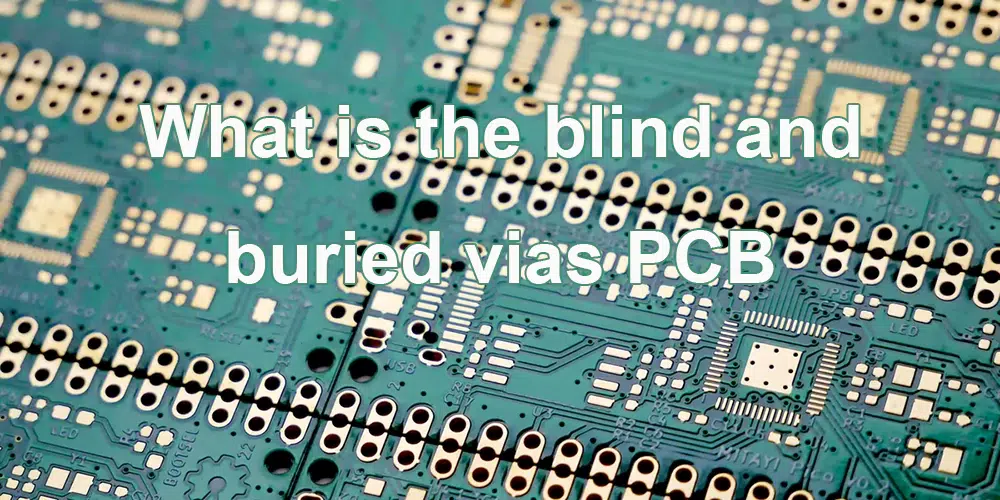
The role of blind & buried vias PCB
1.Improve circuit board integration
Blind and buried via technology can add more connection points to the board, which reduce noise and electromagnetic interference in the board, and improve the reliability and stability of the board. In addition, Blind and buried vias PCB can also achieve a large number of connections, making the space use of the board more efficient and reducing the cost of the board.
2. Improve signal transmission quality
Blind and buried via technology can achieve high-quality signal transmission between different layers, avoiding signal intercoherence and errors. It can also reduce the length of the signal lines in the board, thereby reducing the resistance and inductance of the signal lines, improving the quality and transmission speed of the signal in the board.
3. Avoid board breakage
Blind and buried hole technology can make the circuit board have better mechanical substrate strength. They can pass the wires directly through the board to enable the different layers to be connected, thus avoiding interruptions caused by excessive pressure or vibration on the board.
The difference between Blind & buried vias PCB and traditional PCB board
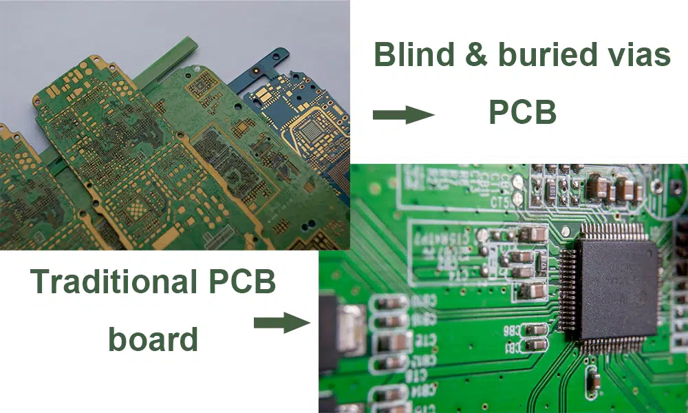
1.The structure is different
Traditional PCB board is a simple copper foil connection in single or multiple layers, with connection points on both sides of the board; The Blind and buried vias PCB adopts a multi-layer PCB board structure, and more connection points are added through blind or buried hole technology on one or both sides of the board to achieve a more efficient connection.
2. The functionality is different
Traditional PCB boards are mainly used to connect circuits, which play the role of fixing and isolating circuits to a certain extent; In addition to connecting circuits, Blind and buried vias PCB can also realize functions such as high-speed signal transmission, noise reduction, and transmission efficiency improvement.
3. The process is different
Blind and buried vias PCB needs to process the PCB board first, and then punch blind holes or buried holes on the PCB board; The traditional PCB board does not have this step, only copper foil manufacturing is required.
Blind and buried vias PCBs are a more powerful and better circuit board manufacturing technology. Its application can improve the integration of the circuit board, signal transmission quality and protection level, thereby improving the reliability and stability of the circuit board, and is one of the circuit board technologies with application advantages.

Conclusion
Blind and buried vias PCB plays a critical role in the performance and stability of electronic products, which can reduce signal interference, increase board density and number of holes, improve the stability of electronic products, and so on. With the continuous innovation and development of electronic products, Blind and buried vias PCB will undoubtedly become a new direction for future development in the field of electronic product manufacturing.

