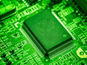
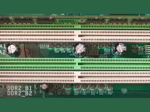
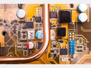
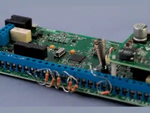
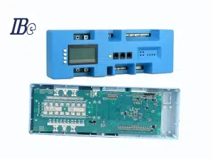
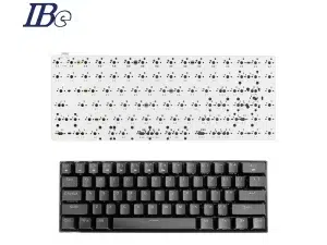
The electronic manufacturing industry encompasses a wide range of products and fields, including electronic materials such as monocrystalline silicon, polycrystalline silicon, semiconductor discrete devices, integrated circuits, etc.; manufacturing of electronic components and equipment such as discrete devices, integrated circuits, capacitors, resistors, inductors, display devices, lithium batteries, connectors, electro-acoustic devices, etc.; consumer and industrial products such as mobile phones, microcomputers, tablet computers, communication equipment, etc.
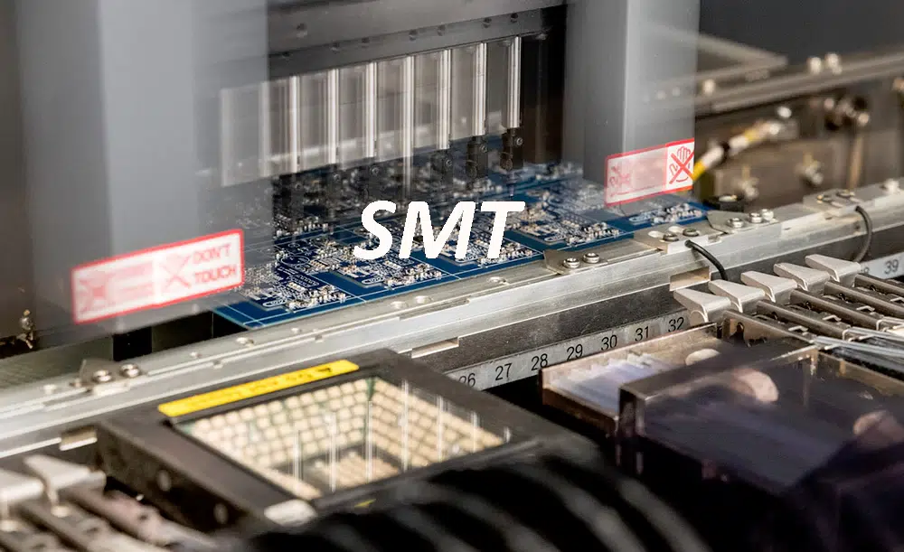
1. SMT (Surface Mount Technology)
– Surface Mount Technology, a manufacturing process where electronic components are directly mounted onto the surface of a printed circuit board (PCB).
2. PCB (Printed Circuit Board)
– Printed Circuit Board, used to support and connect electronic components in circuits.
3. DIP (Dual In-line Package)
– Dual In-line Package, a common form of electronic component packaging.
4. SMD (Surface Mount Device)
– Surface Mount Device, electronic components suitable for SMT processes.
5. BGA (Ball Grid Array)
– Ball Grid Array, a high-density packaging technology.
6. IC (Integrated Circuit)
– Integrated Circuit, a device that integrates multiple electronic components onto a single chip.
7. PCB Assembly
– The process of assembling electronic components onto a PCB.
8. Reflow Soldering
– A soldering process where components are soldered to a PCB by melting solder paste through heating.
9. AOI (Automated Optical Inspection)
– Automated Optical Inspection, used to inspect the quality of electronic components and solder joints on PCBs.
10. X-Ray Inspection
– X-Ray Inspection, used to inspect the quality of internal solder joints, such as those in BGA packages.
11. ICT (In-Circuit Test)
– In-Circuit Test, a functional test of electronic components on a PCB.
12. FCT (Functional Test)
– Functional Test, a test of the overall functionality of a PCB or product.
13. THT (Through Hole Technology)
– Through Hole Technology, a process of soldering electronic component leads through holes in a PCB.
14. SMT Line
– SMT Production Line, including equipment such as printers, pick-and-place machines, and reflow ovens used for SMT processes.
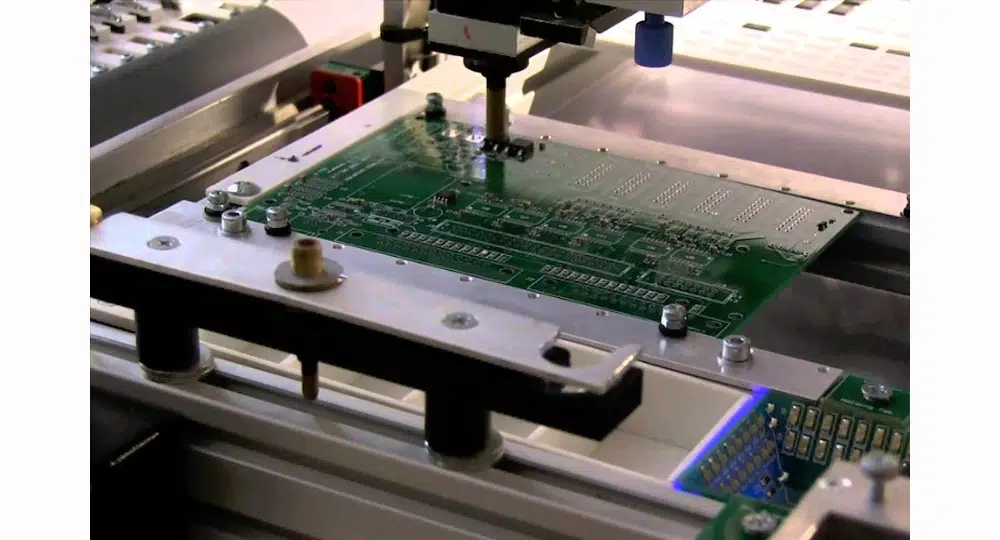
15. Component Mounting
– The process of accurately placing SMD components onto a PCB.
16. Stencil Printing
– Printing solder paste onto a PCB using a stencil.
17. Pick and Place
– Placing SMD components onto a PCB using a pick-and-place machine.
18. Solder Paste
– A mixture of metal powder and flux used to solder SMD components.
19. Lead-Free Solder
– Solder material that does not contain lead, used for environmental reasons.
20. Wave Soldering
– A method of soldering through-hole components on a PCB by passing them over a wave of molten solder.
21. Cleaning
– Removing contaminants and flux residues from a PCB.
22. Quality Control
– Ensuring products meet specified quality standards.
23. Yield
– The ratio of acceptable products to total production.
24. ESD (Electrostatic Discharge)
– Electrostatic discharge, a potential source of damage to electronic components.
25. Reliability
– The ability of a product to perform as intended under specified conditions.
26. PCB Fabrication
– The process of manufacturing PCBs, including design, drilling, etching, etc.
27. Component Lead Forming
– Shaping component leads for soldering or installation.
28. Solder Joint
– The connection point between an electronic component and a PCB.
29. Void
– A bubble or gap within a solder joint that may affect its quality and reliability.
30. PCB Thickness
– The thickness dimension of a PCB board.
31. Copper Thickness
– The thickness of copper foil on a PCB.
32. Impedance Control
– Ensuring signal transmission impedance matches on a PCB.
33. RF PCB
– RF PCB, used for high-frequency signal transmission.
34. Microvia
– Small diameter holes in a PCB.
35. Blind Via
– A hole that connects internal layers of a PCB but does not go through the entire board.
36. Buried Via
– A hole that is completely enclosed within inner layers of a PCB.
37. PCB Material
– Materials used for PCBs, such as FR-4, Rogers, etc.
38. SMT Component Feeder
– Device supplying SMD components to pick-and-place machines.
39. Nozzle
– Pick-and-place machine tool used for picking up and placing SMD components.
40. Feeder Calibration
– Calibration of SMD component feeders to ensure accurate component supply.
41. Component Placement Accuracy
– Precision in placing components by pick-and-place machines.
42. Reflow Profile
– Temperature profile in a reflow oven that affects soldering quality.
43. Solderability
– The ability of electronic component pins or PCB pads to be soldered.
44. PCB Flux
– Chemical substance used to facilitate soldering.
45. Solder Spatter
– Splattering of solder particles during soldering.
46. Tombstoning
– Vertical standing of SMD components due to uneven soldering.
47. Component Shift
– Deviation of component position after placement compared to design.
48. PCB Warpage
– Bending or deformation of a PCB.
49. SMT Production Line
– Overall process flow of SMT production, including printing, component placement, reflow soldering, etc.
50. Cycle Time
– Time required to complete one production cycle.
51. SMT Stencil
– Stencil used for printing solder paste in SMT.
52. Adhesive
– Material used to secure SMD components on a PCB.
53. Component Packaging
– The appearance and pin arrangement of electronic components.
54. QFN (Quad Flat No-Lead)
– Surface mount package with no leads on its sides.
55. SOP (Small Outline Package)
– Common type of integrated circuit package.
56. SOJ (Small Outline J-lead Package)
– Small outline package with J-shaped leads.
57. PLCC (Plastic Leaded Chip Carrier)
– Plastic package for integrated circuits.
58. PGA (Pin Grid Array)
– Package with pins arranged in a grid pattern.
59. COB (Chip-on-Board)
– Mounting method where chips are directly mounted on a PCB.
60. Wire Bonding
– Method of connecting chips to a PCB or substrate.

61. Flip Chip
– Chip mounted face-down on a PCB or substrate.
62. Underfill
– Material used to fill the gap between a chip and PCB for enhanced reliability.
63. PCB Design
– Includes layout, routing, signal integrity considerations, etc.
64. Gerber File
– Graphic file format used for PCB manufacturing.
65. DFM (Design for Manufacturing)
– PCB design method considering manufacturing processes.
66. NPI (New Product Introduction)
– Process of introducing a new product into production.
67. BOM (Bill of Materials)
– List of materials needed for production.
68. MOQ (Minimum Order Quantity)
– Minimum quantity suppliers require for orders.
69. JIT (Just-in-Time)
– Production method where parts are produced as needed.
70. Kanban
– Signal system for controlling production flow.
71. Cost of Goods Sold
– Direct costs incurred in producing goods.
72. ROI (Return on Investment)
– Measure of investment profitability.
73. ERP (Enterprise Resource Planning)
– Integrated management system for business processes.
74. MES (Manufacturing Execution System)
– Real-time monitoring and management of production processes.
75. Six Sigma
– Quality management method aiming to reduce defects and improve process stability.
More electronic terms/terminologies will be updated…

