Demystifying PCB Schematic Diagram : Understanding the Basics

Demystifying PCB Schematic Diagram : Understanding the Basics

A PCB schematic diagram is a visual representation of an electronic circuit using standardized symbols and connections. It illustrates how components are interconnected to form a functional electronic system. This diagram acts as a blueprint for the PCB layout design and eventual manufacturing.

PCB schematic diagrams are crucial in the electronics design and manufacturing process, serving as a visual guide and documentation for building electronic circuits.

Table of Contents

What is a PCB schematic diagram?

A PCB (Printed Circuit Board) schematic diagram is a graphical representation of an electronic circuit. It illustrates the connections and relationships between various electronic components using standardized symbols. The schematic diagram provides a blueprint for the PCB layout, aiding in the design and assembly process.

It typically includes symbols representing components like resistors, capacitors, integrated circuits, connectors, power sources, and more. These symbols are connected by lines indicating how these components are electrically connected within the circuit.

What is the importance of PCB using the schematic diagram?

The importance of using a schematic diagram in PCB design is multi-faceted:

• Design Visualization: Schematics provide a visual representation of the circuit’s structure, helping designers understand the relationships between components, their connections, and how the circuit functions. It offers a clear blueprint before actual implementation.

• Component Placement: Schematics guide the placement of components on the PCB. By understanding how components are interconnected, designers can strategically place them to optimize the board’s layout for efficiency and functionality.

• Wiring Guidance: Schematics indicate how components should be connected and help determine the routing paths for traces on the PCB. This ensures that signals flow correctly, minimizing interference and maximizing efficiency.

• Documentation and Communication: Schematics serve as documentation for the circuit’s design. They provide a standardized way to communicate the circuit’s details to other team members, engineers, or technicians involved in the design, testing, or troubleshooting phases.

• Troubleshooting Aid: When issues arise during testing or assembly, the schematic acts as a reference for diagnosing problems. Engineers can trace connections and identify potential faults, making troubleshooting more efficient.

• Consistency and Reproducibility: Schematics ensure consistency in circuit design. They provide a standardized format for circuit representation, making it easier to reproduce the design or modify it for different versions or similar circuits.

In summary, using a schematic diagram in PCB design is crucial for understanding, planning, implementing, and troubleshooting electronic circuits, ensuring accurate and efficient PCB layouts that function as intended.

What is the difference between a PCB layout and a PCB schematic diagram?

Difference between a PCB layout and a PCB schematic diagram

A PCB schematic diagram and a PCB layout serve distinct purposes in the design and fabrication of a printed circuit board (PCB):

PCB Schematic Diagram:

Function: The schematic diagram provides a visual representation of the electrical connections between components in a circuit.

Components: It illustrates the relationships between various components, their symbols, pin connections, and how they are interconnected.

Purpose: Schematics are primarily used for conceptualizing, designing, and understanding the circuit’s functionality.

Software: Created using schematic design software, it focuses on logical representation rather than physical layout.

Details: It includes component values, part numbers, annotations, and netlists (the connections between components).

PCB Layout:

Function: The layout refers to the physical arrangement of components and their interconnections on the actual PCB.

Components: It defines the precise locations, orientations, and interconnection paths of components on the board.

Purpose: PCB layout is used for translating the schematic into a physical design suitable for manufacturing.

Software: Designed using PCB layout software, it includes detailed component placement, routing of traces, ground planes, power distribution, and manufacturing specifications.

Details: The layout specifies the physical dimensions, trace widths, layers, vias, and other details necessary for fabricating the PCB.

In essence, a schematic provides a conceptual view of the circuit’s electrical connections and component relationships, while the PCB layout translates that concept into a physical design with precise component placement and routing on the actual board. Both are crucial stages in the PCB design process, each serving a specific purpose in bringing the electronic circuit from concept to reality.

What does a PCB schematic contain?

A PCB schematic contains essential information about the electronic circuit being designed. It typically includes:

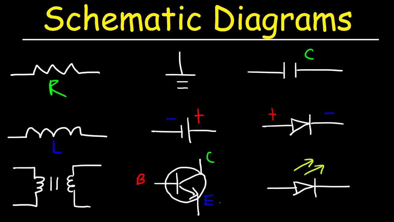
Component Symbols: Symbols representing various electronic components like resistors, capacitors, diodes, transistors, integrated circuits, etc.

Component Identifiers: Designators or labels that uniquely identify each component in the circuit. These are usually alphanumeric (e.g., R1 for resistor 1, C2 for capacitor 2).

Connections and Nets: Lines or wires representing connections between component pins. Nets show how components are electrically connected in the circuit.

Component Values: Values or specifications of components, such as resistance values for resistors, capacitance values for capacitors, part numbers, etc.

Power and Ground Symbols: Symbols indicating power supply connections and ground points within the circuit.

Netlist: A list specifying how each component pin is connected to other pins. It’s essential for understanding the electrical connectivity of the circuit.

Annotations and Comments: Information added by the designer, including notes, comments, annotations, or descriptions for clarity and documentation.

Designators and Pin Numbers: Designators show which components are which on the schematic, while pin numbers correspond to the physical pins on the components.

Functional Blocks: For complex circuits, functional blocks or modules help in organizing and understanding different sections of the circuit.

Overall, the PCB schematic provides a detailed and organized representation of the circuit’s electrical connections, component relationships, and specifications necessary for designing the physical PCB layout and for manufacturing the circuit.

What does a PCB schematic contain?

How do you design a PCB schematic diagram?

Designing a PCB schematic diagram involves several steps:

1. Identify Requirements: Understand the functionality, components, and connections needed for your circuit. Define specifications and constraints.

2. Select Design Software: Choose PCB design software such as Altium Designer, KiCad, Eagle, or OrCAD. Familiarize yourself with the software’s interface and tools.

3. Create a New Project: Initiate a new project in your chosen software. Define the project parameters, including board size, layers, and specifications.

4. Component Selection: Identify and add components from the software library to your schematic. Ensure these components match the requirements of your circuit.

5. Place Components: Arrange the components logically on the schematic sheet. Group related elements together, considering signal flow and connectivity.

6. Wire Connections: Use wiring tools to establish connections between components. Properly label connections and ensure correct signal paths.

7. Label Components and Nets: Add labels and annotations to components and nets to maintain clarity and ease of understanding.

8. Annotate and Organize: Assign reference designators (component identifiers) to ensure unique identification. Organize components systematically for easy referencing.

9. Create Ground and Power Planes: Designate ground and power nets appropriately, ensuring their connectivity and integrity throughout the schematic.

10. Verify and Validate: Perform a thorough review of the schematic for errors, missing connections, or incorrect components. Use design rule checks (DRC) and simulation tools if available.

11. Generate Schematics Documentation: Generate necessary documentation, such as Bill of Materials (BOM) and schematic prints, for manufacturing and assembly.

12. Collaborate and Review: Share your design with peers or experts for feedback. Incorporate suggestions or revisions as needed.

13. Iterate and Improve: Refine the schematic design based on feedback and any identified shortcomings.

14. Final Checks: Perform a final review and check for completeness, accuracy, and adherence to design guidelines.

15. Export Files: Save and export the final schematic files in the required format for further PCB layout design and manufacturing.

Remember, practicing with the chosen software and regularly referencing design guidelines and standards will enhance your proficiency in creating effective PCB schematic diagrams.

Best software for PCB schematic diagram

What is the best software for PCB schematic diagram?

Altium Designer: Known for its comprehensive features, user-friendly interface, and extensive library of components.

Cadence Allegro: Offers powerful functionalities for complex designs, particularly in high-speed applications.

KiCad: An open-source software with a robust set of tools suitable for both hobbyists and professionals.

OrCAD: Known for its versatility, providing a range of tools for schematic capture and layout design.

Eagle PCB: Popular for its simplicity and widespread use in hobbyist and small-scale projects.

PADS: Offers intuitive tools for schematic design and is known for its integration with other tools in the design process.

When choosing software, consider factors like your level of expertise, the complexity of the design, compatibility with other software or systems, support, community resources, and budget constraints. Testing different software options through free trials or demos can help identify the most suitable one for your specific requirements.

What is the format of PCB schematic file?

PCB schematic files can be stored in various formats, each associated with specific PCB design software. Some common formats include:

.SCH (Schematic File): This is a common format used by many PCB design software to save schematic diagrams. Each software may have its own proprietary format for schematic files (e.g., .SCHDOC in Altium Designer).

.BRD (Board File): While this primarily refers to the PCB layout file, it often contains elements of the schematic, especially in integrated design software where the schematic and layout are closely tied together.

.DXF (Drawing Exchange Format): DXF files are often used for exchanging vector-based drawings, and they might contain PCB schematics or components.

.PDF (Portable Document Format): PDFs can also store PCB schematics, usually as exports from the original design software.

.ASC (ASCII File): Some PCB design software allows for exporting schematics in ASCII format, which can be easily read and edited using text editors or other software.

The specific format used often depends on the software used to create and edit the schematic diagrams.

Conclusion

In summary, using a schematic diagram in PCB design is crucial for understanding, planning, implementing, and troubleshooting electronic circuits, ensuring accurate and efficient PCB layouts that function as intended.

FAQ

A PCB (Printed Circuit Board) schematic diagram is a graphical representation of an electronic circuit. It illustrates the connections and relationships between various electronic components using standardized symbols.

Component Symbols

Component Identifiers

Connections and Nets

Component Values

Power and Ground Symbols

Netlist

Annotations and Comments

Designators and Pin Numbers

Functional Blocks

Altium Designer

Cadence Allegro

KiCad

OrCAD

Eagle PCB

PADS

Leave a Comment

Your email address will not be published. Required fields are marked *

HOW CAN WE HELP YOUR BUSINESS?

From engineering design, to prototype, manufacturing and beyond — IBE is your trusted ecosystem partner that can scale and enable your complex technology solutions.