Printed Circuit Boards (PCBs) are the backbone of modern electronic devices, facilitating the interconnection of electronic components to create functional circuits. While the focus often lies on the intricate network of copper traces and the protective solder mask, another critical element quietly plays its part on the surface of the PCB – the PCB silkscreen.
The silkscreen layer is not involved in the actual electrical function of the circuit but is crucial for the manufacturing, assembly, and servicing of the PCB. It helps ensure that components are placed correctly, facilitates troubleshooting, and provides necessary information about the board’s specifications and usage.
What is a silkscreen in PCB ?
PCB silkscreen refers to the layer of markings, symbols, text, and graphics that are printed onto the surface of a printed circuit board. These markings are typically in white (though other colors can be used) and provide essential information for the assembly, testing, and maintenance of the PCB. PCB Silkscreen is applied over the solder mask layer and is visible on both the top and bottom sides of the PCB.
What are shown on a PCB silkscreen?
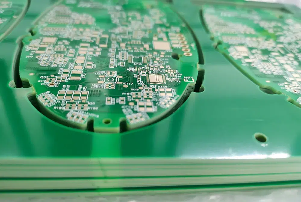
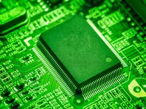
1. Component Outlines and Designators: The PCB silkscreen often includes outlines or footprints of components, showing where each component should be placed during assembly. It may also include component designators (like R1 for resistor 1, C2 for capacitor 2, etc.) to identify each component.
2. Reference Designators: These are alphanumeric codes or labels that uniquely identify each component on the PCB. They help during assembly, testing, and troubleshooting.
3. Polarity Markings: For components like diodes, LEDs, and electrolytic capacitors, polarity markings (such as + and – signs) are indicated on the silkscreen to ensure correct orientation during assembly.
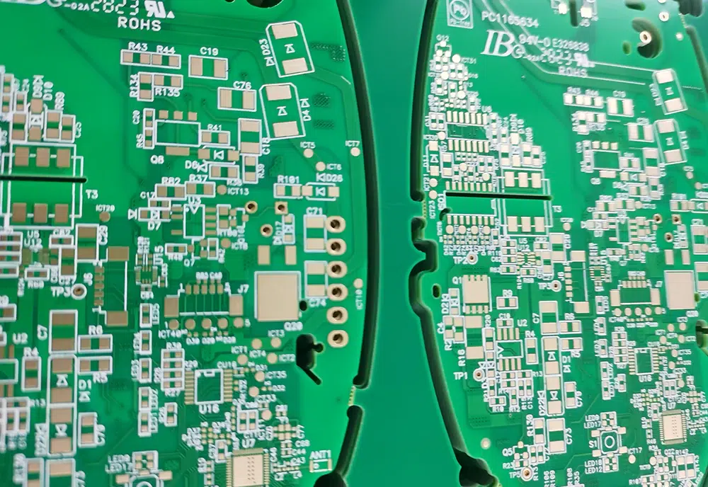
4. PCB Identification: The PCB silkscreen often includes information such as the board part number, revision number, manufacturer logo, and other identifying marks.
5. Assembly Instructions: Some PCBs may have assembly instructions or guidelines printed on the silkscreen to aid technicians during assembly and testing processes.
6. Safety Warnings and Notes: Depending on the application, important warnings, notes, or symbols related to safety or operational requirements may be included on the PCB silkscreen.
What is the difference between solder mask and silkscreen ?
Solder mask and silkscreen are both essential elements of a printed circuit board (PCB), but they serve different purposes and are applied to different layers of the PCB:
| Solder Mask | PCB Silkscreen | |
|---|---|---|
| Purpose | The solder mask, also known as solder resist, is a layer of polymer applied to the surface of the PCB to protect the copper traces and pads from oxidation and to prevent solder bridges during assembly. | The PCB silkscreen is a layer of markings, text, symbols, and logos that are printed on the surface of the PCB to convey information related to component placement, assembly instructions, and PCB identification. |
| Material and Color | It is typically green in color (though other colors like red, blue, black, etc., are also used) and is made of a liquid photoimageable epoxy or ink that is cured under UV light. | It is typically white in color (though sometimes other colors are used) and is made of ink that is printed on top of the solder mask layer. |
| Function | The primary function of the solder mask is to insulate copper traces and pads from accidental contact with solder during soldering. It also helps to protect the PCB from environmental factors like dust and moisture. | The PCB silkscreen provides essential information for PCB assembly and maintenance, including component outlines, reference designators, polarity markings, board identifiers, and sometimes assembly instructions or warnings. |
| Application | Solder mask is applied to both sides of the PCB and covers the entire surface except where solder pads and vias are exposed for soldering. | PCB Silkscreen is applied on top of the solder mask layer, so it does not cover the entire PCB surface. Instead, it is selectively printed where markings are needed, such as around component footprints and along the edges of the board. |
How is silkscreen printing done on PCB ?
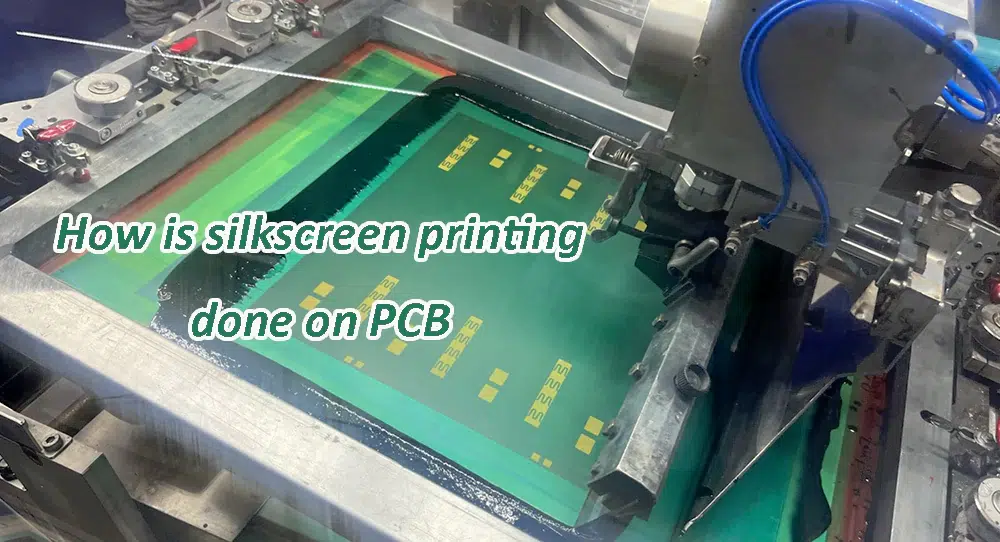
Silkscreen printing on a PCB involves a process similar to traditional screen printing but adapted for the specific requirements of printed circuit boards. Here’s a simplified outline of how silkscreen printing is typically done on a PCB:
1. Preparation of Artwork:
– The silkscreen information, including component outlines, reference designators, logos, and other markings, is prepared digitally using PCB design software. This artwork is typically in vector format to ensure clarity and precision.2. Film Generation:
– The digital artwork is used to generate films (also known as photomasks) that will be used to create the screens for printing. Each layer of the silkscreen design (typically top and/or bottom) requires its own film.
3. Screen Preparation:
– Screens are prepared by coating a fine mesh screen with a light-sensitive emulsion. This emulsion is exposed to UV light through the film containing the silkscreen artwork. Areas exposed to UV light harden, while areas blocked by the artwork remain soft.
4. Developing the Screen:
– After exposure, the screen is washed with water, causing the unexposed (soft) emulsion to dissolve and wash away, leaving behind a stencil on the screen corresponding to the silkscreen artwork.
5. Setup on the Printing Machine:
– The prepared screens are then mounted onto a printing machine designed for PCBs. The PCB itself is securely held in place on the printing table, usually by vacuum suction, to ensure accurate alignment.
6. Ink Application:
– Ink is applied onto the screen. A squeegee blade then presses the ink through the stencil onto the PCB surface. The ink passes through the open areas of the stencil (where the emulsion was washed away), transferring the silkscreen design onto the PCB.
7. Curing the Ink:
– Once the silkscreen printing is complete, the PCB may pass through a curing process where the ink is dried or cured under UV light or through heat, depending on the type of ink used.
8. Inspection and Quality Control:
– After curing, the PCB is inspected to ensure the silkscreen markings are clear, accurate, and aligned correctly with the PCB features. Any defects or inconsistencies may require rework.
9. Final Processing:
– After silkscreen printing, the PCB may proceed to other manufacturing steps such as solder mask application, component placement, soldering, and testing.
This process ensures that the silkscreen information, which is crucial for component placement, identification, and assembly instructions, is accurately and durably applied to the PCB surface. The precision of silkscreen printing contributes to the overall quality and functionality of the printed circuit board.
How thick is the PCB silkscreen ?
The primary purpose of the silkscreen is to provide markings, text, symbols, and logos that aid in the assembly, identification, and maintenance of the PCB.
The PCB thickness of the silkscreen is controlled during the screen printing process. The amount of ink deposited onto the PCB surface is carefully managed to ensure that the PCB silkscreen markings are clear and legible without being excessive.
The relatively thin nature of the PCB silkscreen helps to maintain the overall flatness and dimensional accuracy of the PCB surface.
Typical PCB Thickness Range:
– PCB silkscreen thickness typically falls within the range of 10 to 50 micrometers (μm), which is 0.01 to 0.05 millimeters (mm).
This thickness is relatively thin compared to other layers on the PCB, such as the copper layers or solder mask.
What are the colors of PCB silkscreen ?
PCB silkscreen is primarily available in several standard colors, though white is the most commonly used. The choice of color can vary depending on the PCB manufacturer, specific requirements of the design, or aesthetic preferences. Here are the typical colors of PCB silkscreen:
* White:
White is the most common color for PCB silkscreen. It provides good contrast against the green solder mask (which is also very common) and makes the markings and symbols easily readable.
* Black:
Black silkscreen is also used, especially when a contrasting color is preferred against a lighter-colored solder mask (such as green or yellow). Black silkscreen can provide a sleek and professional appearance.
* Other Colors:
In addition to white and black, other colors may be available depending on the PCB manufacturer’s capabilities and the specific requirements of the design. These colors can include red, blue, yellow, or even custom colors specified by the customer.
What is the line width for PCB silkscreen?
The line width for PCB silkscreen (also known as silkscreen resolution or feature size) typically depends on the capabilities of the PCB manufacturer and the specific requirements of the design. Here are some general guidelines:
Minimum Line Width:
* The minimum line width for PCB silkscreen is typically in the range of 5 to 10 mils (thousandths of an inch), which translates to approximately 0.127 to 0.254 millimeters.
* Some manufacturers may specify even finer resolutions, down to 4 mils (0.1 mm) or less, especially for detailed text and symbols.
Recommended Line Width:
* A recommended line width for PCB silkscreen is around 7 to 8 mils (0.178 to 0.203 mm). This width ensures that the silkscreen markings are clear and legible, even after the PCB undergoes processes such as solder mask application and component assembly.
In summary, while there is flexibility in the line width for PCB silkscreen, a minimum line width of around 5 to 10 mils (0.127 to 0.254 mm) is common, with a recommended width of approximately 7 to 8 mils (0.178 to 0.203 mm) for optimal visibility and manufacturability. Designers should work closely with PCB manufacturers to ensure that silkscreen requirements align with manufacturing capabilities and achieve the desired visual clarity on the final printed circuit board.
What is the IPC standard for PCB silkscreen ?
• IPC-2221: “Generic Standard on Printed Board Design”
– This standard provides guidelines for the design of printed circuit boards, including considerations for component placement, labeling, and marking, which indirectly influence silkscreen requirements.
• IPC-7351: “Generic Requirements for Surface Mount Design and Land Pattern Standard”
– Although primarily focused on land pattern designs for surface mount components, it includes considerations for component outlines and designators that are relevant to silkscreen markings.
• IPC-2612: “Sectional Requirements for Electronic Diagramming Symbol Generation Methodology”
– This standard provides guidelines for creating electronic diagrams and symbols, which can be referenced for the creation of silkscreen symbols and markings.
IPC-A-600: “Acceptability of Printed Boards”
– This standard covers acceptance criteria for printed circuit boards, including criteria related to markings, labeling, and legends, which indirectly influence silkscreen requirements.
How do you remove PCB silk screen ?
Removing PCB silkscreen, whether partially or completely, can be necessary in certain situations such as rework, design changes, or refurbishing. Here are some methods commonly used to remove PCB silkscreen:
1. Mechanical Methods:
– Scraping: Using a sharp tool or a scraper, gently scrape off the silkscreen markings from the PCB surface. This method requires careful control to avoid damaging the underlying solder mask or copper traces.
2. Chemical Methods:
– Chemical Solvents: Various solvents can be used to dissolve or soften the silkscreen ink. Common solvents include acetone, isopropyl alcohol (IPA), and specialized ink removers.
– *Acetone:* Acetone is effective for removing many types of ink, but it should be used with caution as it can also affect the solder mask or other materials on the PCB.
– *Isopropyl Alcohol (IPA):* IPA is less aggressive than acetone and is safer to use, but it may require longer soaking times and multiple applications.
– *Specialized Ink Removers:* There are commercial products specifically designed for removing silkscreen ink from PCBs. These products are formulated to be effective yet gentle on the PCB materials.
3. Heat and Abrasion:
– Heat Gun: Applying heat using a heat gun can soften the silkscreen ink, making it easier to scrape off. Care must be taken to avoid overheating the PCB and causing damage.
– Abrasive Methods: In some cases, abrasive methods such as sanding or using abrasive pads may be used to mechanically remove silkscreen. However, these methods can also scratch or damage the PCB surface, so they are less commonly used.
4. Laser Ablation:
– Laser technology can be used to selectively remove silkscreen markings from PCBs. This method is precise and avoids damage to surrounding areas, but it requires specialized equipment and expertise.
Conclusion
In summary, PCB silkscreen plays a vital but often overlooked role in the production and functionality of printed circuit boards. From guiding component placement to providing crucial identification and assembly instructions, silkscreen ensures that electronic devices are assembled correctly and operate reliably. As technology advances and electronic devices become more complex, the importance of clear and precise silkscreen markings only grows, making it an indispensable component in modern electronics manufacturing.
PCB silkscreen refers to the layer of markings, symbols, text, and graphics that are printed onto the surface of a printed circuit board. These markings are typically in white (though other colors can be used) and provide essential information for the assembly, testing, and maintenance of the PCB.
Component Outlines and Designators
Reference Designators
Polarity Markings
PCB Identification
Assembly Instructions
Safety Warnings and Notes
Preparation of Artwork
Film Generation
Screen Preparation
Developing the Screen
Setup on the Printing Machine
Ink Application
Curing the Ink
Inspection and Quality Control
Final Processing

