In the ever-evolving landscape of electronics, Printed Circuit Board Assembly (PCBA) stands as the backbone of innovation and technological progress.
The assembly of intricate electronic components onto a well-designed circuit board not only symbolizes the convergence of hardware and software but also embodies the meticulous craftsmanship that underlies our interconnected world.
This article serves as a gateway into the realm of PCBAs, exploring the types, components, process, and the testing that ensure the reliability and functionality of these vital electronic components.
1. Fundamentals of PCB Assembly
PCBA is a versatile and integral process that enables the creation of diverse electronic devices, contributing to advancements in technology, automation, and connectivity across various sectors.
1.1. What is PCB Assembly?
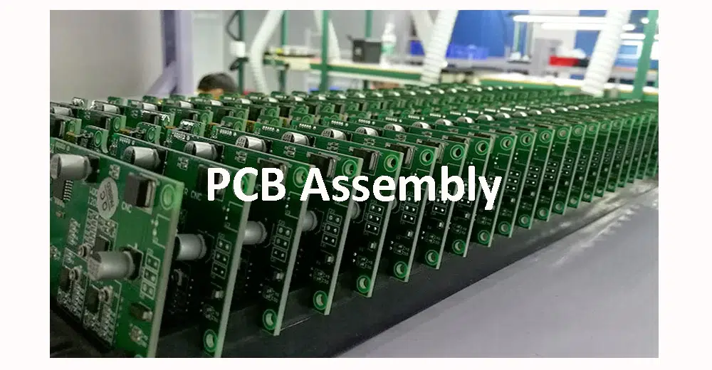
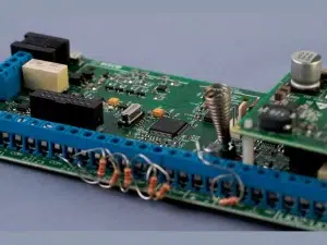
At its core, PCB Assembly is the process of populating a printed circuit board (PCB) with electronic components to create a functional electronic device. The PCB acts as a platform that connects and supports these components, facilitating the flow of electrical signals to achieve the desired functionality.
1.2. What are the types of PCB?
PCBs come in various types, each designed to cater to specific applications. The most common types include single-sided PCBs, double-sided PCBs, multi-layered PCBs, flexible PCB, rigid-flex PCB, and HDI PCB. The choice of PCB type depends on the complexity of the electronic device and the desired performance.
1.3. what are the components of a PCB?
Understanding the basic components of a PCB is essential for grasping the assembly process. Key elements include:
a. Substrates: The base material of the PCB, typically made of fiberglass-reinforced epoxy.
b. Copper Traces: Thin conductive paths that connect different components and facilitate the flow of electrical signals.
c. Solder Mask: A protective layer that covers the PCB, preventing unintentional electrical connections and ensuring component alignment during assembly.
d. Silkscreen: Identifies components and provides additional information like polarity and component values.
2. What are the key electronic components in PCBA?
In PCBA, various electronic components play crucial roles in creating functional electronic devices. These components can be broadly categorized into active and passive components, each serving a specific function. Here are key electronic components commonly used in PCBA:
2.1. Active Components
Integrated Circuits (ICs): ICs are miniature electronic circuits that integrate multiple components onto a single chip. They serve as the core processing units in electronic devices, providing functions such as amplification, signal processing, and logic operations.
Microcontrollers and Microprocessors: These components are specialized ICs that contain a central processing unit (CPU), memory, and input/output peripherals. Microcontrollers are commonly used in embedded systems, while microprocessors are the brains of computers and other computing devices.
Transistors: Transistors are semiconductor devices that amplify or switch electronic signals. They come in various types, including bipolar junction transistors (BJTs) and field-effect transistors (FETs), and are fundamental to electronic circuits.
Diodes: Diodes allow current to flow in one direction only, acting as rectifiers in power supplies or as semiconductor devices in signal processing circuits. Light-emitting diodes (LEDs) are a common type of diode that emits light when current flows through it.
Operational Amplifiers (Op-Amps): Op-amps are versatile integrated circuits used for amplifying and processing analog signals. They find applications in amplifiers, filters, and various analog signal processing circuits.
2.2. Passive Components
Resistors: Resistors limit the flow of electric current and are essential for controlling voltage levels, biasing circuits, and providing load resistance. They come in various resistance values and power ratings.
Capacitors: Capacitors store and release electrical energy. They are used for smoothing voltage, filtering signals, and providing energy storage in electronic circuits. Capacitors come in different types, including electrolytic, ceramic, and tantalum capacitors.
Inductors: Inductors store energy in a magnetic field when current flows through them. They are used in applications such as filtering, energy storage, and inductive coupling. Inductors are typically coils of wire wound around a magnetic core.
Resistor Networks and Arrays: These are integrated circuits that contain multiple resistors in a single package. They simplify the assembly process and are often used in applications where multiple resistors with the same value are needed.
Crystals and Oscillators: Crystals and oscillators generate precise clock signals for timing and synchronization in electronic circuits. They are crucial in applications such as microcontrollers, microprocessors, and communication systems.
2.3. Connectors
Pin Headers and Sockets: Pin headers are used to provide electrical connections between the PCB and other components, such as cables or additional boards. Sockets are receptacles that allow easy insertion and removal of components, such as ICs.
Edge Connectors: These connectors are located at the edge of the PCB and facilitate connections with other boards or external devices. They are commonly used in applications like memory modules and expansion cards.
Ribbon Connectors: Ribbon connectors consist of flat cables with multiple conductors that can be connected to PCBs using connectors. They are often used in applications where space is a consideration.
2.4. Power Supply Components
Voltage Regulators: Voltage regulators maintain a stable output voltage regardless of variations in input voltage or load. They are crucial for providing a consistent power supply to sensitive components.
Transformers: Transformers are used to step up or step down voltage levels in power supply circuits. They consist of two or more coils wound around a magnetic core and are essential for AC-DC conversion.
These key electronic components form the building blocks of PCBA, allowing for the creation of sophisticated and functional electronic devices across various industries. The proper selection, placement, and integration of these components are critical for the reliable and efficient operation of the final electronic product.
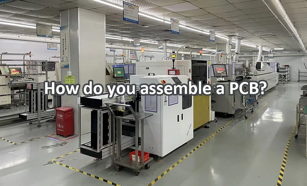
3. How do you assemble a PCB?
3.1. Steps of PCB Assembly
PCBA involves a series of carefully orchestrated steps to transform a bare printed circuit board (PCB) into a functional electronic device. The process can vary slightly depending on factors such as the type of components used, the assembly method (surface mount technology or through-hole technology), and the complexity of the PCB design. Here are the general steps involved in PCBA:
1. Component Placement:
Automated or Manual Placement: Depending on the scale of production, components can be placed on the PCB manually or using automated pick-and-place machines.
Component Libraries: The PCB layout, which includes the locations for each component, is created using electronic design automation (EDA) tools. Component libraries within these tools store information about each component’s footprint, orientation, and value.
2. Solder Paste Application:
Stenciling: A stencil is placed over the PCB, and solder paste is applied through the openings in the stencil onto the solder pads. The solder paste serves as a temporary adhesive for holding components in place before soldering.
3. Pick-and-Place:
Automated Component Placement: Automated pick-and-place machines use vision systems to precisely pick up components and place them onto the solder paste on the PCB.
Component Verification: Machine vision systems or manual inspection may be used to verify that each component is correctly placed.
4. Reflow Soldering:
Heating and Melting: The entire PCB is subjected to a controlled heat source in a reflow oven. This melts the solder paste, creating a permanent electrical and mechanical connection between the components and the PCB.
Cooling: The PCB is then cooled to solidify the solder joints.
5. Inspection:
Automated Optical Inspection (AOI): AOI machines use cameras and image recognition algorithms to inspect the PCB for defects, including misaligned components, missing components, and solder joint issues.
X-ray Inspection: X-ray machines may be used to inspect hidden solder joints or components beneath surface-mounted devices.
Manual Inspection: Skilled technicians may perform additional manual inspections to ensure the quality of the assembly.
6. Through-Hole Component Insertion (if applicable):
Automated or Manual Insertion: For PCBs that use through-hole components, these components are inserted into pre-drilled holes either manually or using automated insertion equipment.
Wave Soldering (if applicable): The PCB is passed over a wave of molten solder, which solders the through-hole components to the PCB.
7. Second Reflow (if applicable):
Double-Sided Assembly: In cases where components are placed on both sides of the PCB, a second reflow process may be necessary to solder the components on the second side.
8. Cleaning (if applicable):
Flux Residue Removal: Flux residues from soldering processes can be cleaned using various methods, such as ultrasonic cleaning, to improve the appearance and reliability of the final assembly.
9. Conformal Coating (if applicable):
Protective Coating: PCBA may require a conformal coating to protect against environmental factors such as moisture, dust, and chemical exposure.
10. Testing:
Functional Testing: The PCBA undergoes functional testing to ensure that it operates according to specifications.
In-Circuit Testing (ICT): ICT involves checking individual components and connections on the PCB to identify any defects or issues.
11. Packaging and Final Inspection:
Packaging: The assembled and tested PCBs are packaged for shipping or integration into the final product.
Final Inspection: A final inspection may be conducted to ensure that the assembled PCBs meet quality standards before being shipped to customers.
The successful execution of these steps requires precision, attention to detail, and adherence to industry standards to produce reliable and high-quality PCBA. Automated equipment, advanced inspection technologies, and skilled personnel all contribute to the efficiency and accuracy of the PCBA process.
3.2. Surface Mount Technology (SMT) vs. Through-Hole Technology (THT)
PCBA involves two primary assembly methods: Surface Mount Technology (SMT) and Through-Hole Technology (THT). SMT components are mounted directly onto the surface of the PCB, while THT components have leads passing through holes in the board. The choice between SMT and THT depends on factors such as component size, complexity, and cost considerations.
4. What is different PCB and PCBA?
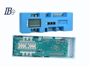
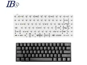
A PCB is a rigid board with electronic components and copper traces connecting them. It serves as a foundation for electronic devices. On the other hand, PCBA refers to the complete assembly process, including soldering components onto the PCB. While a PCB is the bare board, PCBA represents the finished product with mounted and soldered electronic components, ready for use.
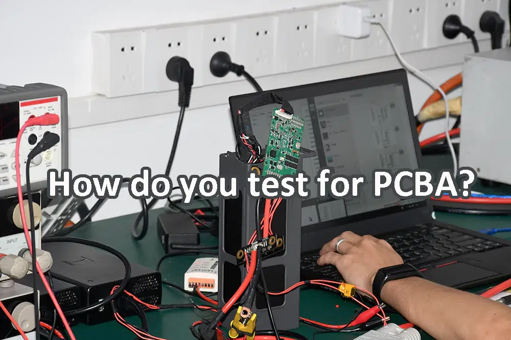
5. How do you test for PCBA?
PCBA Testing is a crucial step in the electronics manufacturing process to ensure quality and reliability. Various testing methods are employed to identify defects, ensure functionality, and meet the required specifications. Here are some common testing techniques for PCBA:
1. Visual Inspection:
Conduct a visual inspection to identify issues such as soldering defects, component misplacement, and physical damage.
2. Automated Optical Inspection (AOI):
AOI systems use cameras and image processing algorithms to automatically inspect the PCBA for defects, including solder joint quality and component placement.
3. In-Circuit Testing (ICT):
ICT involves testing individual components and connections on the PCB to ensure that they meet the specified electrical characteristics. This method is effective for identifying issues such as shorts, opens, and incorrect component values.
4. Functional Testing:
Functional testing verifies that the PCBA performs its intended functions. This can be done using test fixtures and specialized equipment that simulates real-world operating conditions.
5. Boundary Scan Testing (JTAG):
Joint Test Action Group (JTAG) testing uses a standardized interface (IEEE 1149.1) to test and debug digital circuits on the PCB. It is particularly useful for identifying faults related to interconnections and logic errors.
6. X-ray Inspection:
X-ray inspection is used to check hidden solder joint quality, identify defects in BGA (Ball Grid Array) packages, and ensure proper component alignment.
7. Thermal Testing:
Thermal testing involves subjecting the PCBA to temperature variations to identify potential thermal issues, such as overheating or inadequate heat dissipation.
8. Burn-In Testing:
Burn-in testing involves operating the PCBA at elevated temperatures for an extended period to identify latent defects that may surface under stress.
9. Environmental Testing:
Environmental testing exposes the PCBA to various environmental conditions, such as temperature extremes, humidity, and vibration, to ensure that it can withstand different operating conditions.
10. Insulation Resistance Testing:
This test measures the resistance between conductive elements to identify any insulation breakdowns or leakage.
Conclusion
From the design phase to the exhaustive testing processes, every facet of PCBA creation is a testament to the commitment of engineers, manufacturers, and quality control professionals to deliver excellence.
With about 20 years experience, IBE Electronics is a professional PCBA/ODM/OEM manufacturer. We provide one-stop service including electronic design, manufacturing, prototype, components, assembly and testing. Choose us as your ODM/OEM manufacturer for unparalleled expertise, innovative design, and one-stop production solutions.

