Many packaging choices are appropriate for semiconductor devices. Based on the shape, size and structure of the package, it can be divided into three types that are pin insertion type, surface mount type and advanced packaging.
Semiconductor products are developing from two-dimensional to three-dimensional. From the direction of technological development, new packaging methods such as system-in-package (SiP) have appeared. From the technical realization method, flip chip, bumping, wafer advanced packaging technologies such as wafer level package, 2.5D packaging (interposer, RDL, etc.), 3D packaging (TSV), etc.
Traditional Packaging vs Advanced Packaging
Traditional packaging began to emerge after the initial triode in-line period. Its process is as follows: After the wafer is cut into dies, the dies are attached to the corresponding lead frame pads of the substrate frame, and then the bonding pads of the chips are connected to the wind bonds of the substrate.
It realizes the electrical connection and finally protects it with a shell (mold, or encapsulation). Typical packaging methods include DIP, SOP, TSOP, QFP, etc.
Advanced packaging mainly refers to flip chip, bumping, wafer level package, 2.5D packaging (interposer, RDL, etc.), 3D packaging (TSV) and other packaging technologies.
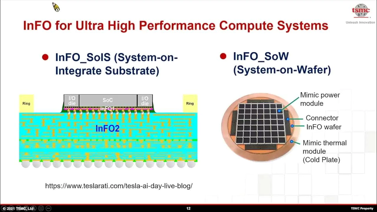
Advantages of advanced packaging
1. Improve processing and design efficiency, and reduce design costs.
Taking wafer-level packaging as an example, products are mass-produced in the form of wafers. Existing wafer preparation equipment can be utilized, and package design can be performed at the same time as chip design. It shortens the design and production cycle and reduces costs.
2.Improve packaging efficiency and reduce product costs.
With the advent of the post-Moore’s Law era, traditional packaging is hard to meet the needs. The packaging efficiency (bare core area/substrate area) of traditional packaging is low, and there is a lot of room for improvement. When the chip manufacturing process is limited, improving packaging is another way out.
3.Driven by higher efficiency, lower cost, and better performance.
Advanced packaging technology appeared in the 1990s. By realizing electrical interconnection in the form of dot-strip lines, higher-density integration can be achieved, which greatly reduces the waste of area.
SiP technology and PoP technology have laid the beginning of the advanced packaging era, 2D integration technologies, such as wafer level packaging, flip-chip, and 3D packaging technology, through silicon via, etc.
The emergence of technology further reduces the connection distance between chips and improves the response speed of components, which will continue to promote the development of advanced packaging in the future.
Also read: Guide to BGA chip soldering process
Advanced Packaging Technology
Flip-Chip & Bumping
Flip chip
It refers to chip flipping. In the past packaging technology, the active area of the chip is facing up, facing away from the substrate and bonding after bonding. While flip chip faces the active area of the chip to the substrate, and realizes the interconnection between the chip and the substrate through the solder bumping arranged in an array on the chip.
The silicon chip is directly installed on the PCB in an upside-down manner, and the I/O is drawn from the silicon chip to the surroundings.
The interconnection length is greatly shortened, the resistance-capacitance delay is reduced, and the electrical performance is effectively improved.
The advantages of flip chip are mainly in the following points:
- Small size
- Enhanced function (increased number of I/O), performance (short interconnection), improved reliability (flip chip can reduce the number of interconnection pins by 2/3)
- Improved heat dissipation (the back of the chip can be effectively cooled)
Bumping
Bumping is a new type of electrical interconnection between chips and substrates.
It can be achieved by using small spherical conductive materials, which are called bump. The process of making conductive balls is called bumping. When the die with bump is inverted and aligned with the substrate, the die is easily connected to the substrate pad. Compared with traditional wire connection, flip-chip has many advantages, such as smaller package size and faster device speed.
Also read: FC-CSP (flip-chip chip scale package) – a comprehensive guide for beginners
2.5D Packaging: RDL & Interposer
RDL (Redistribution layer)
At the wafer level, contact redistribution can be performed very efficiently. The redistribution layer is used to re-plan the connection path, fall to the desired area, and obtain a higher contact density. The process of redistribution actually adds one or more layers to the original wafer.
First, a layer of dielectric is deposited for isolation, then we will expose the original contacts, and then deposit a new metal layer to achieve re-layout. UBM will be used here to support solder balls or contact balls of other materials.
Interposer
It refers to the conductive layer between the solder ball and the grain. Its role is to expand the connection surface, so that a connection can be redirected to where we want. Similar to the role of the redistribution layer.
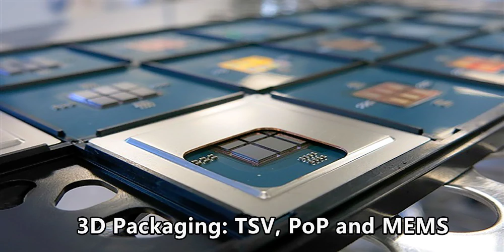
3D Packaging: TSV, PoP and MEMS
TSV (Through-silicon via)
Bump and RDL will occupy the plane area where the chip is bonded to the substrate, and TSV can stack the chips to make use of the three-dimensional space. More importantly, the stacking technology improves the electrical properties when connecting multiple chips.
Wire bonding can be used for stacking technology, but TSV is more attractive. TSV realizes the electrical connection throughout the thickness of the chip, and opens up the shortest path between the upper and lower surfaces of the chip. Shorter lengths of connections between chips also mean lower power consumption and greater bandwidth.
PoP (Package on Package)
PoP is a packaging technology that combines separate logic and storage BGA packages in the vertical direction. In this structure, more than two layers of packaging units are stacked together from bottom to top, leaving a dielectric layer in the middle to transmit signals.
PoP technology increases the integration density of the device, and the bottom packaging unit is directly in contact with the PCB board. Traditional PoP is based on substrate stacking. With the demand for high bandwidth of memory, the space between balls is required to be smaller. In the future, it will be combined with FOWLP technology to make chip-based stacking.
MEMS packaging
Micro-electromechanical systems have become more and more widely used in recent years. With the large-scale implementation of sensors and Internet of Things applications, MEMS packaging has also attracted much attention. The packaging of MEMS is different from the packaging of integrated circuits. It is divided into multiple vertical hierarchical packaging such as chip level, module level, card level, board level, and gate level.
FIWLP & FOWLP, PLP
First of all, the concept of wafer-level packaging should be mentioned. In the traditional packaging concept, the wafer is first cut into small dies, and then connected and molded. The wafer-level packaging process is just the opposite. Wafer-level packaging completes the packaging of the die before being cut, the protective layer will be attached to the front or back of the wafer, and the circuit connection has been completed before cutting.
FIWLP
Fan-in wafer-level packaging that is, traditional wafer-level packaging, cutting the die at the end, suitable for low pin count integration circuit.
As the number of pins for integrated circuit signal output increases, the size of solder balls becomes more and more strict. The PCB’s adjustment requirements for the size of the integrated circuit package and the position of the signal output pins fail to be met, so derivatives out of fan-out wafer-level packaging. Fan-in wafer-level packaging is characterized by a package size that is the same size as the die.
FOWLP
Fan-out wafer-level packaging. The die is cut at the beginning, and then redistributed on a new artificially molded wafer. Its advantage is that it reduces the thickness of the package, increases the fan-out (more I/O interfaces), and obtains better electrical properties and better heat resistance.
FIWLP and FOWLP have different purposes, and both are the mainstream packaging methods in the future. FIWLP is the most widely used in analog and mixed-signal chips, followed by wireless interconnection, and CMOS image sensors are also packaged with FIWLP technology. FOWLP will primarily be used in processor chips in mobile devices.
PLP
Panel-level packaging. Its packaging method is similar to FOWLP, except that the grains are reorganized on larger rectangular panels instead of round wafers. A larger area means more cost savings and higher packaging efficiency.
Moreover, the cut die is square, and the wafer packaging will result in waste of corner area, and the rectangular panel just solves the waste problem. But it also puts forward higher requirements for lithography and alignment.
1.Improve processing and design efficiency, and reduce design costs.
2.Improve packaging efficiency and reduce product costs.
3.Driven by higher efficiency, lower cost, and better performance.
- Small size
- Enhanced function, performance, improved reliability
- Improved heat dissipation
Flip chip, bumping, wafer advanced packaging technologies such as wafer level package, 2.5D packaging (interposer, RDL, etc.), 3D packaging (TSV), etc.

