PCB impedance refers to the resistance of an electric circuit on a printed circuit board (PCB) to alternating current. Impedance is a critical parameter that affects signal quality and integrity in high-speed digital circuits.
As technology advancements, PCBs with high-density interconnects become more common, resulting in higher operating frequencies and tighter constraints on signal timing. Therefore, understanding and controlling the PCB impedance becomes increasingly important as it can lead to signal distortion, electromagnetic interference, and ultimately system failure.
Designers must consider various factors such as trace width, spacing, and material properties during layout and routing to ensure accurate impedance matching across all circuits on the board. This will improve signal transmission, reduce noise, and enhance overall system performance.
What is the PCB impedance
PCB impedance refers to the resistance of a printed circuit board (PCB) to electrical current flow, particularly when alternating currents are applied. Impedance is affected by various factors such as PCB width, thickness, and distance between copper coils. It is an important consideration in designing and manufacturing PCBs for high-frequency applications, as it affects signal quality and transmission efficiency. An impedance-controlled PCB ensures that signals move reliably and with minimal loss.

What are the types of impedance
There are two types of impedance:
1. Resistance – This is a measure of how much a material or circuit resists the flow of electric current through it.
2. Reactance – This is a measure of how much an electrical component such as a capacitor, inductor, or transformer impedes the flow of alternating current (AC) through it.
Why is PCB impedance control required
PCB impedance control is required in order to ensure the reliable and efficient functioning of high-speed digital circuits.
Modern electronic devices such as computer motherboards, mobile phones and server systems require high data transmission rates, along with consistent signal quality, for optimal performance.
Impedance refers to the resistance that an electrical circuit imposes on the flow of alternating current (AC) at a specific frequency.
The presence of impedance can cause reflections and noise in high-frequency signals which can degrade its amplitude or phase over distance. This means signals may be incorrectly received by nearby components or transmitted out, even leading to damage of electronics if it gets worse without correction.
To avoid this issue, PCB designers include impedance control techniques in board layout designs to maintain uniform electrical characteristics through various circuit layers. With precise measurement and calculation methods, they specify appropriate trace widths, spacing and via design parameters to achieve desired impedance values.
What are the factors that affect PCB impedance
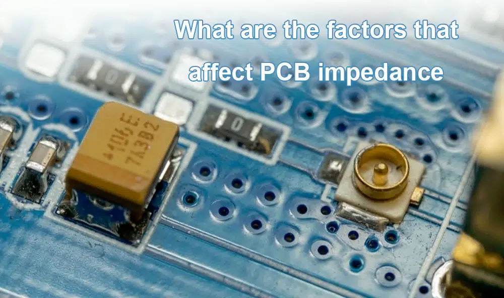
1. PCB trace geometry: Trace width, thickness, height from ground plane, curvature, and length affect impedance.
2. Dielectric constant of PCB material: The dielectric constant of the substrate affects the propagation speed of the signal on the PCB. A higher dielectric constant leads to lower characteristic impedance.
3. Distance between traces and planes: The distance between signals and return paths can impact the electrical behavior of the system entirely.
4. Frequency of operation: Higher frequency design necessitates tighter tolerance control for characteristic impedance with shorter signal rise/fall times.
5. Component placement: Component location may not only disrupt the routing of signal traces but also will cause stray capacitance & inductance to arise between purposeful circuits.
6. Temperature: The increase or decrease in temperature influences the features such as thermal expansion/contraction causes changes in resistance values of conductor materials which in turn impact the characteristics of impedance.
7. Copper roughness: Copper roughness is a measurement of copper surface irregularity determines how much microstrip resonator performance gets affected.
8. Via design: Maintain a trajectory that guarantees fundamental resonance immune routing to minimize unnecessary time delays at via portion.
How to design PCB impedance
1. Determine the type of signal being transmitted through the trace (analog, digital, RF) and its frequency range.
2. Define the characteristic impedance requirement based on the signal type and frequency range. The most common values are 50Ω and 75Ω for RF signals, and 100Ω and 120Ω for digital signals.
3. Set the allowed tolerance for impedance variation along the trace length. Common values are ±10% and ±20%.
4. Decide on the stack configuration of your PCB, as this can affect the trace impedance. The thickness and dielectric constant of each layer will determine the effective width and spacing of the trace.
5. Calculate the physical dimensions of the trace using a PCB design tool such as Altium or Eagle. There are several online calculators that can assist with these calculations as well.
6. Simulate the electrical performance of the trace using software such as CST Studio Suite, Ansys HFSS, or Keysight ADS. This will give you an accurate prediction of the trace impedance and any potential reflections or attenuation.
7. Adjust the trace dimensions until the simulated impedance is within the desired tolerance range. Repeat the simulation with different parameters if necessary.
What is PCB board selection
PCB board selection refers to the process of choosing a suitable printed circuit board (PCB) for a specific electronic application or project. When selecting a PCB board, factors such as size, shape, number of layers, thickness, material, and other specifications should be considered in order to ensure that the board meets the requirements of the intended application. The right PCB board choice can impact the.
How to calculate PCB impedance

1. Open your PCB design software and create a new project or open an existing one.
2. Draw the PCB traces or routes that carry signals between components.
3. Define the layer stack-up for your circuit board. This includes identifying the number of layers, copper thicknesses, dielectric materials used, and their respective thicknesses.
4. Specify the signal trace width, height, and spacing based on your desired impedance value.
5. Use the built-in calculator in the PCB design software to compute the impedance of each signal trace based on its dimensions and the layer stack-up parameters.
6. Confirm that the computed impedance values meet the required specifications for your application.
7. Adjust the trace width, height, and spacing as necessary until you achieve the desired impedance values.
8. Save your design and generate the Gerber files needed for manufacturing.
Tools for calculating PCB impedance
1. Online calculators: There are numerous online calculators available that allow you to input the parameters of your PCB design and calculate its impedance.
2. PCB design software: Many PCB design software packages include built-in impedance calculators that can help you analyze your designs and optimize the trace widths and spacing to achieve a desired impedance.
3. Signal integrity analysis tools: Advanced signal integrity analysis tools like Ansys HFSS, CST Microwave Studio, and ADS can provide in-depth simulation of complex PCB structures and accurately predict their impedance behavior.
4. Reference materials: There are many PCB design guides and textbooks available that provide tables and equations for calculating the characteristic impedance of various PCB structures.
5. Manufacturer datasheets: Most PCB manufacturers provide datasheets that include detailed information about the characteristic impedance of their materials and recommended stackup configurations.
Considerations for high-speed PCB design
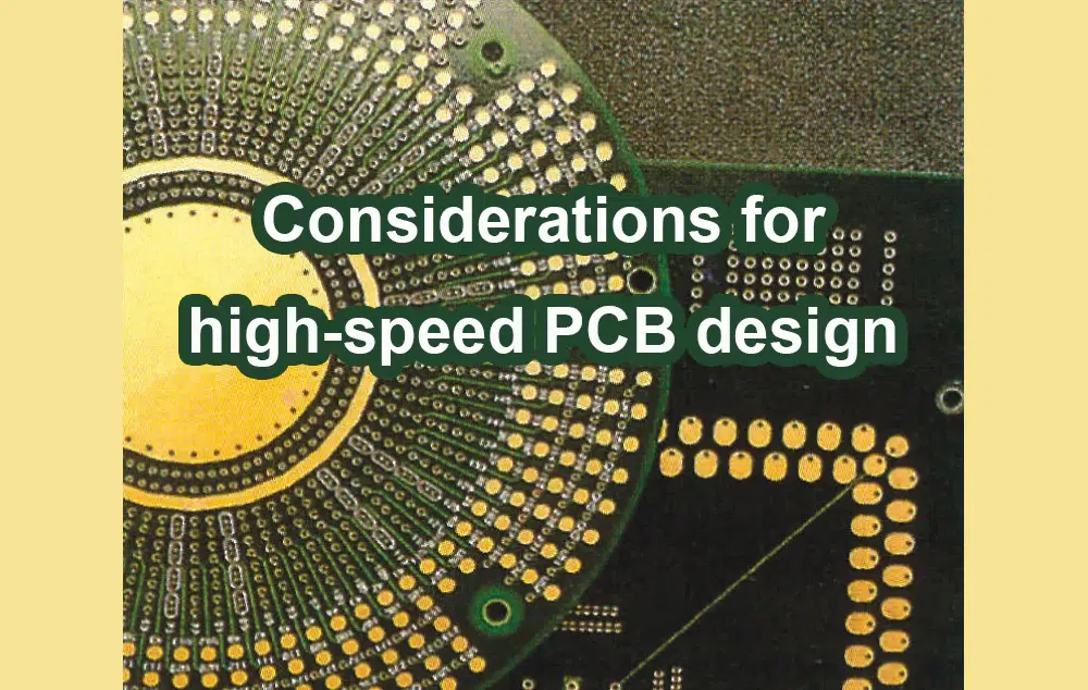
1. Signal Integrity: High-speed designs require careful consideration of signal integrity, including impedance control, crosstalk, and termination techniques.
2. Power Delivery: High-speed PCBs may have demanding power requirements that need to be carefully managed, such as voltage ripple, current stability, and thermal management.
3. Layer Stackup: The layer stackup determines the overall performance of the high-speed PCB design. It needs to be optimized for minimizing signal loss, reducing crosstalk, and managing heat dissipation.
4. Component Placement: It is essential to place components strategically in order to minimize trace length, reduce parasitic capacitance, and improve signal integrity.
5. Routing: Careful attention should be given to routing rules, including trace width, spacing, and via placement. Controlled-impedance routing must be used wherever required.
6. Material selection: Choosing materials with appropriate dielectric constant (Dk) values, low-loss tangent, and suitable thickness can ensure improved signal transmission and reduced signal distortion.
7. EMI/EMC considerations: High-speed designs are prone to electromagnetic interference (EMI) and electromagnetic compatibility (EMC) issues. Proper shielding, grounding, and filtering should be taken into account during the design process.
8. Testing and Validation: Rigorous testing and validation processes are essential to verify the proper functioning of high-speed PCBs under different operating conditions and environments. Advanced simulation tools and test equipment can facilitate this process.
Conclusion
In conclusion, PCB impedance plays a critical role in determining the performance and reliability of electronic circuits. Impedance matching ensures that signals propagate efficiently and without distortion, leading to better signal integrity and reduced signal loss.
Proper design practices such as controlled trace width and spacing, proper ground plane layouts, and selection of appropriate materials can help achieve desirable impedance values and minimize variations due to manufacturing processes.
Careful consideration of PCB impedance is crucial for high-speed and high-frequency applications such as telecommunications, networking, and multimedia, where even small deviations from target impedances can severely impact system performance.

