Wire bonding, a fundamental process in semiconductor packaging and electronic assembly, serves as the backbone for establishing electrical connections between integrated circuits (ICs) or semiconductor devices and the printed circuit board (PCB). From smartphones and laptops to automotive electronics and medical devices, wire bonding quietly enables the seamless transmission of signals.
What is wire bonding in PCB?
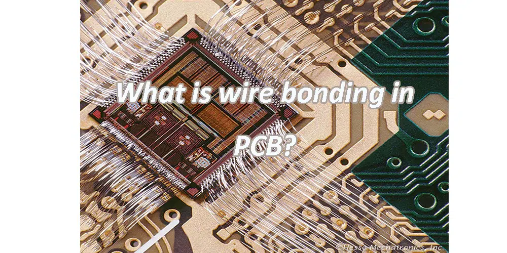
Wire bonding in PCB (Printed Circuit Board) manufacturing is a technique used to connect integrated circuits (ICs) or semiconductor devices to the PCB substrate. It involves creating electrical connections between the ICs and the PCB by using very fine wires made of materials like gold, aluminum, or copper.
Wire bonding is a crucial step in the manufacturing of many electronic devices, as it allows for the creation of reliable electrical connections between ICs and the PCB, enabling the device to function as intended.
Why do we use wire bonding?
Wire bonding is used in PCB manufacturing for several reasons:
Reliability: Wire bonding creates strong, reliable electrical connections between ICs and the PCB substrate. These connections are essential for the proper functioning of electronic devices and ensure that signals can be transmitted accurately.
Miniaturization: Wire bonding allows for the creation of very small electrical connections, which is crucial for modern electronic devices that are becoming increasingly compact and lightweight. The fine wires used in wire bonding can be precisely placed, enabling manufacturers to pack more functionality into smaller spaces.
Cost-effectiveness: Compared to alternative methods such as flip-chip bonding, wire bonding tends to be a more cost-effective solution, particularly for applications where high-density packaging is not required.
Compatibility: Wire bonding is compatible with a wide range of semiconductor materials and packaging types, making it a versatile choice for various electronic devices.
Flexibility: Wire bonding can accommodate different bond pad geometries and sizes, allowing for flexibility in PCB design and layout.
Repairability: In case of a defective connection, wire bonding can be repaired relatively easily compared to other bonding methods. This can help reduce scrap and manufacturing costs.
What is the difference between soldering and wire bonding?
Soldering and wire bonding are both methods used in electronic assembly and PCB manufacturing, but they serve different purposes and have distinct processes. Here are the key differences between soldering and wire bonding:
Purpose:
Soldering: Soldering is primarily used to create permanent electrical and mechanical connections between components and the PCB. It involves melting solder, a metal alloy, to bond two surfaces together.
Wire Bonding: Wire bonding is used to create electrical connections between integrated circuits or semiconductor devices and the PCB. It involves attaching very fine wires from specific points on the IC to corresponding points on the PCB.
Method:
Soldering: In soldering, solder is melted and applied to the joint between two surfaces (such as a component lead and a PCB pad). The solder solidifies to form a bond, creating both an electrical connection and a mechanical joint.
Wire Bonding: In wire bonding, fine wires (typically made of gold, aluminum, or copper) are physically bonded between the IC and the PCB. This is usually done using heat, pressure, and sometimes ultrasonic energy to create a metallurgical bond between the wire and the bonding pads.
Materials:
Soldering: Soldering typically uses a solder alloy, which is a mixture of metals such as tin and lead or lead-free alternatives like tin-silver-copper (Sn-Ag-Cu). Flux may also be used to clean surfaces and aid in solder flow.
Wire Bonding: Wire bonding uses fine wires made of materials like gold, aluminum, or copper. The choice of wire material depends on factors such as conductivity, corrosion resistance, and cost.
Application:
Soldering: Soldering is used for various applications in electronics assembly, including attaching components to PCBs, soldering wires to terminals, and creating electrical connections on circuit boards.
Wire Bonding: Wire bonding is specifically used to create connections between ICs or semiconductor devices and the PCB. It is commonly used in the assembly of integrated circuits, microchips, and other semiconductor packages.
What material is wire bonding?
Wire bonding typically involves using fine wires made of metals such as:
Gold (Au): Gold wire bonding is common in high-reliability applications due to its excellent electrical conductivity, corrosion resistance, and reliability. It is often used in industries like aerospace, medical devices, and high-end electronics.
Aluminum (Al): Aluminum wire bonding is less expensive compared to gold and is often used in applications where cost is a significant factor. However, aluminum wire bonding may not be as reliable in some environments and can be more prone to corrosion.
Copper (Cu): Copper wire bonding is gaining popularity due to its excellent electrical conductivity and lower cost compared to gold. Copper wire bonding can provide good performance in many applications but may require additional processing steps to prevent oxidation and ensure bond reliability.
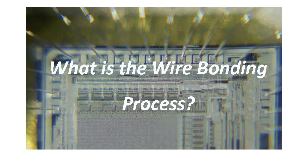
What is the Wire Bonding Process?
Preparation:
● The ICs and PCB are prepared, ensuring that their surfaces are clean and free from contaminants.
● Bonding pads on the IC and corresponding pads on the PCB are cleaned and prepared for bonding.
Alignment:
● The IC is carefully aligned and positioned on the PCB using automated machinery to ensure precise placement.
● Vision systems may be used to verify alignment accuracy.
Wire Selection:
The appropriate wire material and diameter are selected based on the specific requirements of the application.
Wire Bonding:
● Fine wires are bonded from specific points (bonding pads) on the IC to corresponding points on the PCB.
● Wire bonding is typically performed using automated wire bonding machines.
● There are two main methods of wire bonding:
a. Ball Bonding:
● A small ball of wire is formed at one end of the wire.
● The ball is pressed onto the bonding pad on the IC.
● Heat and pressure are applied to create a metallurgical bond between the wire and the pad.
b. Wedge Bonding:
A wedge-shaped tool is used to bond the wire directly to the bonding pad on the IC.
Heat and pressure are applied to create a bond between the wire and the pad.
Ultrasonic Bonding:
● In both ball bonding and wedge bonding, ultrasonic energy is often used to aid in bonding.
● Ultrasonic energy helps to create a strong and reliable bond between the wire and the bonding pad.
Testing:
● Once the wire bonding process is complete, the PCB is typically tested to ensure that all connections are functioning correctly.
● This may involve electrical testing to verify continuity and functionality of the bonded connections.
Encapsulation (optional):
In some cases, the bonded ICs may be encapsulated with a protective material such as epoxy to provide mechanical support and environmental protection.
What are the failure modes of wire bonds?
Wire bonds can experience various failure modes, which can affect the performance and reliability of electronic devices. Some common failure modes of wire bonds include:
1. Wire Lift-off or Lifting:
● This occurs when the wire lifts off from the bonding pad or substrate due to inadequate bonding or mechanical stress.
● It can result from factors such as insufficient bonding force, improper bonding parameters, or inadequate surface preparation.
2. Wire Breakage:
● Wire breakage happens when the wire fractures or breaks, resulting in an open circuit.
● It can be caused by mechanical stress, thermal cycling, vibration, or mishandling during assembly or operation.
3. Ball Shear or Wedge Shear Failure:
● Ball shear failure occurs when the ball bond or wedge bond separates from the bonding pad.
● It can result from inadequate bond strength, improper bonding parameters, or substrate defects.
4. Cratering:
● Cratering refers to the formation of craters or voids in the bonding material (typically gold or aluminum) at the interface between the wire and the bonding pad.
● It can occur due to excessive heat, improper bonding parameters, or contamination on the bonding surface.
5. Intermetallic Compound (IMC) Formation:
● IMC formation happens when undesirable compounds form at the interface between the wire and the bonding pad.
● It can lead to reduced bond strength, increased electrical resistance, or corrosion, affecting the reliability of the bond.
6. Aluminum Wire Bonding Reliability Issues:
● For aluminum wire bonding, specific failure modes include aluminum spiking (penetration of aluminum into the semiconductor substrate), wire sweep (formation of loops or arcs in the wire), and aluminum oxide formation (which can degrade bond quality).
7. Environmental Factors:
● Environmental factors such as moisture, temperature extremes, humidity, and chemical exposure can accelerate wire bond failure through corrosion, oxidation, or degradation of bond materials.
What size wire is used for wire bonding?
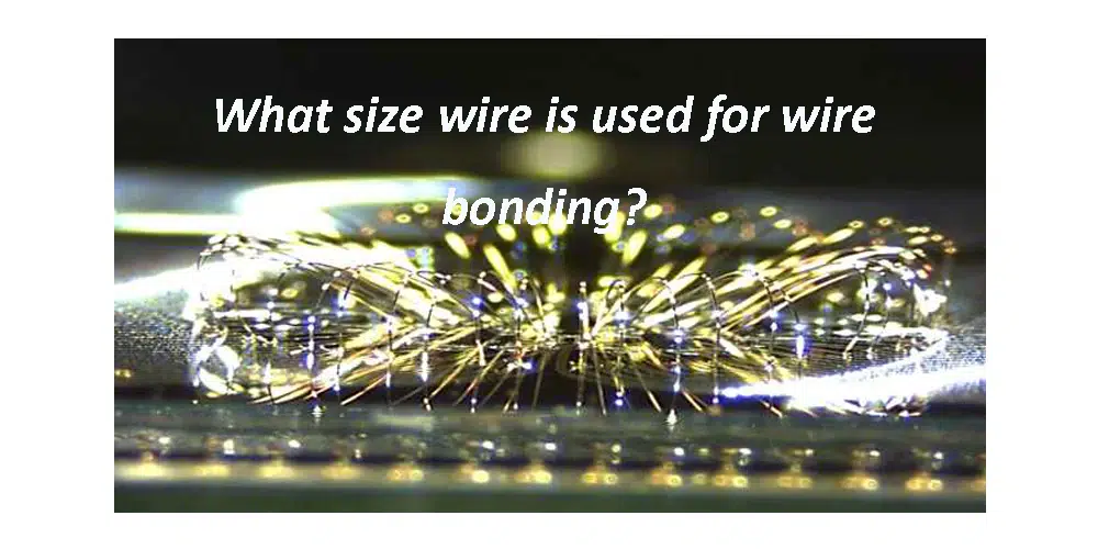
The size of wire used for wire bonding can vary depending on the specific application, package size, and requirements of the electronic device being manufactured. However, wire diameters commonly used in wire bonding typically range from about 10 to 75 micrometers (µm), although finer wires down to 1 µm or coarser wires up to 500 µm can also be used in certain applications.
Here are some common wire diameters used in wire bonding:
Fine Wire Bonding: Wire diameters in the range of 10 µm to 25 µm are commonly used for fine wire bonding applications, especially in high-density packaging and microelectronics.
Standard Wire Bonding: Wire diameters around 25 µm to 50 µm are often used for standard wire bonding applications in semiconductor packaging and integrated circuit assembly.
Heavy Wire Bonding: Wire diameters ranging from 50 µm to 75 µm or larger are typically used for heavy wire bonding applications, such as power devices or applications requiring higher current-carrying capacity.
Conclusion
In the vast landscape of electronics manufacturing, wire bonding stands as a testament to precision engineering and meticulous craftsmanship. As we conclude our exploration of this indispensable technique, it becomes evident that wire bonding is not merely a technical process but a cornerstone of modern technology. Its ability to create reliable electrical connections, withstand harsh operating conditions, and facilitate miniaturization has propelled advancements in semiconductor packaging, enabling the development of ever-smaller, faster, and more reliable electronic devices.

