Printed Circuit board (PCB) is an indispensable part of electronic products, which is the bridge of circuit connection and the carrier of electronic components. In modern electronic technology, PCB has become one of the core components of electronic products. This article will introduce the basic knowledge of PCB: PCB design, manufacturing and assembly, application, etc.
What is the printed circuit board or PCB?
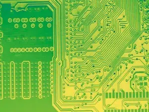
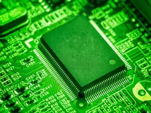
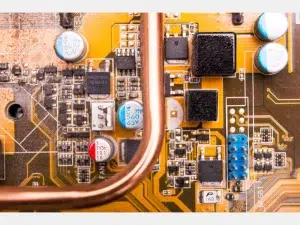
A circuit board, also known as a printed circuit board (PCB), is an important basic component in electronic devices. It acts as a connection and support for electronic components that allow electronic devices to function properly. PCB usually consists of an insulating material as a substrate, coated with a layer of conductive material to form a circuit pattern. On the circuit pattern, electronic components are installed on it by drilling holes and other methods to form a completed circuit.
Are there different types of PCBs?
First, the classification of circuit boards is as follows:
1. Flexible PCB: The printed circuit board made of flexible substrate has the advantage of being able to bend and easy to assemble electrical components. FPC has been widely used in aviation, military, mobile communications, computer peripherals, PDAs, digital cameras and other fields.
2. Rigid PCB: made of paper-based or glass cloth, pre-impregnated phenolic or epoxy resin, the surface adheres to one or both sides of the copper foil, and then laminate and cure; It has a certain rigidity, is not easy to bend, and can be attached to electronic components to provide a certain degree of support.
3. Rigid-flex PCB : laminated together by rigid board and flexible board. The advantage is that it can not only provide the support function of rigid printed plate, but also have the bending characteristics of flexible plate, which can meet the needs of 3D assembly.
Second, the circuit board is divided into the following according to the number of layers:
1. Single side PCB: On the most basic printed circuit board, the parts are concentrated at one end and the wires are concentrated at the other end. Since the wire appears at only one end, this printed circuit board is called single-sided.
2. Double sided PCB: Each end of this circuit board is routed. In order to connect the wires at both ends, an appropriate circuit connection must be made between the two ends, which is called a via, and is used on a more complex circuit than a single panel.
3. Multi-layer PCB: In order to increase the wiringable area, more single-sided or double-sided wiring boards are used, and adhered to each layer after the insulation layer is released, the number of layers on the board represents several independent wiring layers, usually even, and contains the outermost two layers.
Why are PCBs used?
Circuit boards play an important role in electronic products, mainly including the following aspects:
1. Circuit connection: various electronic components are connected on the circuit board by wires, soldering, etc., including integrated circuit chips, resistors, capacitors, inductors, etc. These components are connected together through circuits to form various functional circuits, such as amplification circuits, filter circuits, control circuits, etc.
2. Signal transmission: The circuit board transmits signals between different electronic components through wires and wiring, and realizes signal input, output and processing in electronic products. The wiring design of the circuit board can affect the stability of the signal and the transmission speed, which has an important impact on the performance of the product.
3. Power management: The circuit board usually also includes a power management circuit to manage the power supply and power distribution to ensure that the individual electronic components can work normally. The power management circuitry on the board can include functions such as power switching, voltage regulation, and current protection.
4. Control and processing: In many electronic products, the circuit board also includes core components such as controllers and processors to control and process various signals and data. These control and processing modules are responsible for performing various functions and operations of the product, such as computing, communication, display, sensing, etc.
5. Physical support: Various components and assemblies in electronic products need to have a stable mechanical structure to support and fix, and the circuit board as one of the basic components provides such physical support. It is usually fixed to the casing or the corresponding bracket, ensuring the safety and stability of the individual components.
In summary, circuit boards occupy a key position in electronic products, realizing various functions and features of electronic products through circuit connection, signal transmission, power management, control and processing, and physical support.

Where is PCB used?
1. consumer electronics, such as smartphones, tablets, televisions, etc., the demand for printed circuit boards continues to grow.
2. Industrial control, such as industrial automation, instrumentation, etc., printed circuit boards are widely used.
3. Communication industry, including base stations, satellite communication and wireless communication, is an important application field for printed circuit boards.
4. Medical electronics field, such as medical electrocardiogram, medical ultrasound instrument, medical X-ray machine, etc.
5. PCB is required in the field of automotive electronics, such as electronic control, car navigation, entertainment and security systems.
6. Solar photovoltaics, such as photovoltaic solar panels, photovoltaic inverters, etc.
Please check our IBE website for more information.
What is PCB vs PCBA?
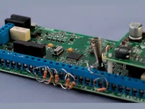
PCBA =PCB+ assembly. Simply put, the PCB is an empty board with only a pattern, while the PCB is a board with various components added. PCB is a pattern based on conductive paths on a non-conductive medium to support and connect electronic components. PCBA, on the other hand, refers to the formation of the structure and function of the circuit by mounting electronic components on the PCB and connecting them. The purpose of PCBA is to assemble different electronic components (such as resistors, capacitors, integrated circuits, etc.) together to achieve specific function circuit boards, which are then widely used in various electronic devices and products, including televisions, mobile phones, computers, household appliances, automotive electronics, etc.
What material is commonly used for PCBs?
The main material of the circuit board is a non-conductive base material, usually a cellulose substrate made of insulating glass fiber cloth. This substrate is called FR-4, and the full name is Flame Retardant 4. FR-4 material has good insulation, mechanical strength and stability, which can meet the needs of most electronic products.
In addition to the base material, the circuit board needs to be covered with a metal conductive layer, usually copper or aluminum. Metal conductive layers can be formed by chemical deposition, plating, etc. to form conductive paths on the circuit board. During the circuit board fabrication process, the conductive layer is usually divided into many different regions, each corresponding to a different circuit element.
When making a circuit board, the base material is first cut to the desired size and a metal conductive layer is applied on it. Then, processes such as photolithography, electroplating, etc. are carried out on the conductive layer to form components such as wires and pads, and excess metal is removed using chemical methods. Finally, the required electronic components are fixed to the circuit board by soldering and other methods to complete the construction of the entire circuit.
The board has many other functions besides connecting and supporting electronic components. For example, multilayer circuit boards can transmit signals between different layers through inner conductive layers, improving the integration and stability of the circuit. In addition, information such as components and traces can be added to the circuit board to facilitate identification and operation during electronics production and repair.
How are printed circuit boards designed?
Here are some basic PCB design steps:
Preliminary preparation:
Preparation of documents such as schematics, block diagrams, footprint libraries, and important design instructions.
PCB structure design:
The netlist is imported → the structure is imported→ the project analysis → module is captured
PCB layout design:
Structural device layout→ key device layout→ modular layout
PCB constraint setting and routing design:
Structural optimization→ cascading design→ rule settings →Class settings
Wiring optimization and silkscreen placement:
Wiring → winding equal length→ power processing→ silkscreen processing
Network DRC inspection and structure inspection:
DRC checks→ project checks→ light plot outputs, and checks → file archives
PCB forming.
How printed circuit boards are manufactured?
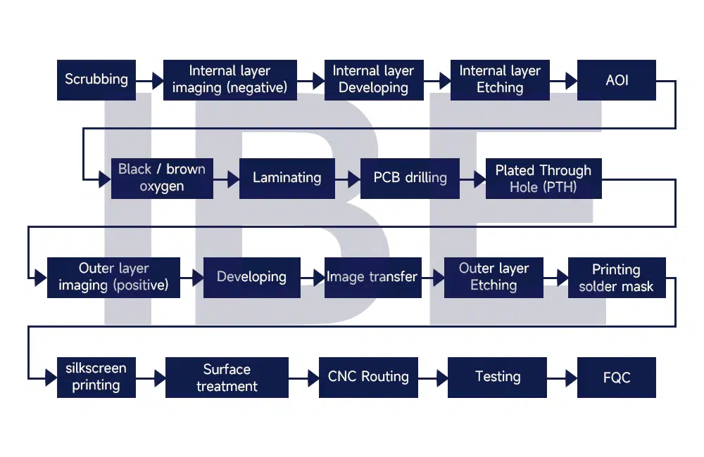
1. Brushing: clean the board surface, remove oxides, etc., and make the clean copper skin and dry film have good adhesion
2. Film: Apply a corrosion-resistant dry film to the surface of the line to be made to protect the copper sheet.
3. Exposure: The light source of the exposure machine passes through the line film film (silver salt film or diazo sheet) transparencies to irradiate the dry film covered by the copper clad laminate to form a pattern.
4. Development: The developer reacts with the dry film that does not polymerize with light, and the compound is detached to expose the copper surface of the copper clad laminate (the copper foil exposed in this similar position will react with the subsequent etching solution to remove the copper foil at such a location), while the dry film that polymerizes with light cannot react with the developer solution and continues to protect the copper foil (and this part of the copper foil is the line that needs to be made).
5. Inner etching: This exposed copper foil is removed by the displacement reaction of the etch solution with the exposed copper foil (which does not need to be made on the conductor part of the board surface) (i.e., the insulating substrate is exposed at this location), while the light-cured dry film does not react with the etching solution and continues to protect the copper foil (which is the part of the copper foil that needs to be made to make the electrical connection performance line).
6. Dedrying film: The dry film that protects the copper foil is fused with an alkaline chemical detergent to exit the dry film covering the copper foil that requires electrical connection performance, presenting the inner bare board route that needs to be made.
7. AOI test: through the inner bare board line produced and the original engineering line data of the CAM design transferred into the AOI instrument for precise spectral scanning comparison, to detect whether there are quality defects such as open circuit, short circuit, line bump, more or less copper skin; and patch line defects in the patchable standard range.
8. Black/Brown:
The inner surface is microscopically roughened to increase the surface contact area and increase the adhesion force of the laminate single during lamination.
9. Lamination:
Under high temperature and high pressure, the layers are bonded into multi-layer boards.
10. Drill:
Make through-hole or laser holes according to the CAM editing and processing of the drilling program file.
11. Porosity (chemical precipitation) PTH:
Copper immersion front brush plate: remove hole burrs and clean the board surface.
Copper immersion: Chemical copper precipitation of the holes, and metallization of the hole walls (connected by the electrical properties of the actual different plate layers)
12. Plating of the whole plate: the copper layer of the perforated wall.
13. Outer light imaging (positive film process):
Brush plate – > film (dry film) – > exposure – > development
14. Pattern transfer (pattern plating):
Brush plate – > degreasing / micro-etching – > electroplated copper – > tinned lead tin / gold plating (positive process) -> etching (de-drying film)
15. Outer etching:
Film removal-> outer line etching (alkaline)-> detinning->QC line inspection-> solder mask (brush plate).
16. solder mask (photosensitive):
Brush plate-> print solder mask-> pre-curing-> exposure-> development-> heat curing-> silkscreen characters.
17. Silk screen characters
Character printing-> hot air curing-> surface treatment.
18. Surface treatment :
Hot air leveling, IMMERSION GOLD, OSP , IMMERSION SILVER, lead-HASL, lead free-HASL
19. Mechanical forming :
CNC Routing
CNC routing machine
Auto registration punch
20. PCB Testing :
E-test
Flying Probe test FPT
Impedance control test system
Microsection analysis
Solderability test
…
21. FQC
How do you assemble a printed circuit board?
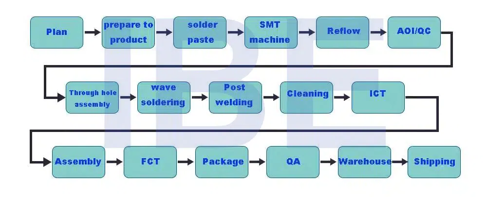
The PCBA production process can be divided into several large processes
(1) PCB manufacturing
(2) After the PCB is completed, the Gerber file is produced, including character layer, line layer, mechanical layer, etc.
(3) Send the Gerber file to the board manufacturer to process the circuit board.
(4) Organize the BOM of components required for PCB boards.
(5) Sort out the component purchase list and submit it to the purchasing department to purchase components.
(6) SMT patch processing: solder paste stirring→ solder paste printing→ SPI → placement→ reflow soldering→AOI → rework.
(7) DIP plug-in processing: plug-in → wave soldering→ foot cutting→ post-welding processing→ plate washing → quality inspection.
(8) PCBA test
(9) Finished product assembly
Conclusion
Founded in 2005, after more than 20 years of innovation and development, IBE group currently has a production base and R&D center in Shenzhen headquarter, EMS&OEM/ODM production base in Vietnam, and a manufacturing base in Fremont EMS in USA. Total area is more than 60,000 square meters, with EVT/DVT/PVT laboratory and EMC test center, high-standard SMT workshop, DIP production line and finished assembly line. With strong manufacturing strength, products are applied in various fields, including laser technology, medical beauty equipment, automotive electronics, industrial control, new energy, sports and entertainment and etc.
Certified by ISO 9001, ISO 14001, UL, IATF16949 , ISO 13485 and etc.
With the rapid changes in the market, in order to effectively shorten the delivery cycle of customers’ goods, IBE Group has strengthened investment in modern equipment, 16 automatic solder-printing machines, 36 high-speed SMT machines, 12 medium and high-speed SMT machines, 12 online SPI, 12 AOI and a series of internationally leading automation equipment. The SMT capacity is up to 50 million chips/day, the plug-in capacity is up to 2 million pieces/day, and the assembly capacity is up to 6 million sets/month. We can mount components including 0201 and 01005, as well as ultra-high-precision QFP, BGA, OPO chips with a pitch of 0.3mm. In addition, we have a modern assembly workshop with 6 complete assembly lines and 2 packaging lines, which can provide customers with finished product assembly for military, medical, aerospace and other industries. With fast delivery cycle and high-quality product, IBE has established good cooperative relations with hundreds of well-known companies around the world, such as Bushnell, VARTA, Valeo, ABB, Grammer and etc., our service scope covers all over the world.

